Continue to Site

Welcome to our site!

Electro Tech is an online community (with over 170,000 members) who enjoy talking about and building electronic circuits, projects and gadgets. To participate you need to register. Registration is free. Click here to register now.

  • Welcome to our site! Electro Tech is an online community (with over 170,000 members) who enjoy talking about and building electronic circuits, projects and gadgets. To participate you need to register. Registration is free. Click here to register now.

net label invisible in Eagle PCB layout

Status
Not open for further replies.

vinodquilon

Member
How can I view net labels on Eagle PCB layout ? Thereby I can easily identify supply & ground nets on the PCB Layout without cross-comparing with its schematic.

I turn-on all the layers in PCB layout, but except net labels all others are visible !!!
 
You place the net labels with either the command 'label' or click on the icon that says label.
 
Actually in my layout layer list $VCC ,$GND layers are not listed.

Hi vinodquilon,

nets can't be labelled in the PCB layout.

Here's what I do to make PCBs userfriendly, labelling connector's nets, e.g. VCC, OUT and GND:

Use the eye symbol and click the desired trace. The net name will be displayed at the left hand bottom of the screen.

Change layer -> tNames(25), change size -> 0.04'' (1.016mm) and Ratio ->6 (normally 8).
Select "Text" and type the text into the window, then place the text where you want it to appear.

You could also use tPlace(21), but disabling tPlace layer will also blank the written text.

Here is an example.

Regards

Boncuk
 

Attachments

  • LABEL..gif
    LABEL..gif
    9.1 KB · Views: 191
Last edited:
Hi Boncuk,

It is very helpful.

There is one more doubt, How we can cross-reference one relay across different sheets. My aim is that, relay is energized by
the circuit in first sheet but its coils act on a different section in another circuit.
 
Hi Boncuk,

It is very helpful.

There is one more doubt, How we can cross-reference one relay across different sheets. My aim is that, relay is energized by
the circuit in first sheet but its coils act on a different section in another circuit.

Hi vinodquilon,

that's an easy one provided the relay is located in one schematic (on a different sheet).

Name the net you want the relay to connect with, e.g. "V+in" and "V+out".

Here is an example switching two different voltages with a DPDT-relay. The NO-terminal nets on sheet one must have the same label as the ones connected anywhere on sheet two.

To make sure the connection is intended Eagle will ask you if they should be connected.

When switching to "board" connections are as given.

Regards

Boncuk
 

Attachments

  • JOIN-01..gif
    JOIN-01..gif
    6.8 KB · Views: 183
  • JOIN-02..gif
    JOIN-02..gif
    4.5 KB · Views: 198
  • JOIN-BRD..gif
    JOIN-BRD..gif
    19.7 KB · Views: 197
component side pcb, comp layout

Hi Boncuk,

One more doubt.
See the three attached files.
.component side pcb, comp layout, my work

First two are done by some other guys in Express PCB and I want 'my work' in Eagle to
convert into both comp side and comp layout sections. How it is possible in Eagle ?
 

Attachments

  • comp layout..PDF
    12.3 KB · Views: 147
  • .component side &#11.PDF
    18.3 KB · Views: 159
  • my work..PDF
    31.7 KB · Views: 192
Component Side & Solder Side

When I auto route, half of the nets comes in the top layer(Component Side) and others in bottom layer(Solder Side).
But I want only components to be placed on top layer. How it is possible ?
Does there any difficulties at PCB manufacturing time due to placing all nets on bottom side ?
 
When I auto route, half of the nets comes in the top layer(Component Side) and others in bottom layer(Solder Side).
But I want only components to be placed on top layer. How it is possible ?
Does there any difficulties at PCB manufacturing time due to placing all nets on bottom side ?

When auto routing you must disable the unwanted layer (top(1)) by clicking until the selection indicates "0" (zero). For the bottom layer select "*", meaning straight and 45 degrees angled traces.

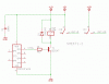
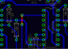
Your design differs a lot from the other one. While there are two ICs on the original design yours has five.

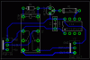
You should see the crossing air wires before routing and rearrange component placement for least crossings.

When routed and there are still unrouted air wires left check thoroughly to give way to a trace.

Using the schematic as reference to place components you're almost done, having the parts on the PCB in a logical order.

A double sided PCB normally requires plated through holes if a component has to be soldered to the through hole.

You can avoid double sided PCBs by planning for wire jumps, connecting two points across another trace. (see screenshot)

Single sided boards are also cheaper to manufacture than double sided ones.

A schematic of "my work" would be much more helpful than a pdf file containing nothing but components (silk screen).

Boncuk
 

Attachments

  • VIA..gif
    VIA..gif
    21.8 KB · Views: 177
Status
Not open for further replies.

Latest threads

Back
Top