Continue to Site

Welcome to our site!

Electro Tech is an online community (with over 170,000 members) who enjoy talking about and building electronic circuits, projects and gadgets. To participate you need to register. Registration is free. Click here to register now.

  • Welcome to our site! Electro Tech is an online community (with over 170,000 members) who enjoy talking about and building electronic circuits, projects and gadgets. To participate you need to register. Registration is free. Click here to register now.

need some explaining about "sliding c class" in hartley oscillator

Status
Not open for further replies.

BkraM

Member
Hi All,

I've been pondering some time about the circuit from the tutorial in the link below and i just cant seem to wrap my head around it:
https://www.learnabout-electronics.org/Oscillators/osc21.php

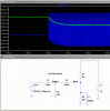
circuit also in picture below:
**broken link removed**

When no oscillations occur it is biased in class A, so Vbe should be about 0.7V which is case (I've build the circuit)
When oscilations start to occur they are amplified by TR1, configured in a common base setup, so that a voltge increase (provided though C2) over R3 results in a increase of Vce and a voltage decrease over R3 in a decrease in Vce.

Apperently during initial oscillations the bias is shifted to that of a C Class amplifier, so Vbe shoul go negative ( which it does in the test circuit).
Here I'm a bit lost, why does this happen?

The site explains it by the large time constant of C2 and R3. I understand the concept of a time constant but can't figure out why this would change the bias of the amp.

Can someone try to explain it to me in some basic steps, or maybe i'm not understanding the common base amp correctly?

Thanks,

I surmise that the polarity of the tank voltage (current) flips once every cycle and that voltage, some of which being fed back to R3 thru the capacitor C2, reverse biases the BE junction of the transistor once every cycle.

And be aware that if the voltage on R3 is greater than the voltage at the base of the transistor, the BE junction IS reverse biased (negative).
 
Last edited:
ccurtis, thanks for your response.

I'm not sure i understand you remark completely, but is the alternating bias though the cycle not just the signal being amplified though TR1 (common base)?

From the tutorial:

"The oscillator in Fig. 2.1.1 uses a common base amplifier. When the oscillator is first powered up, the amplifier is working in class A with positive feedback. The LC tank circuit receives pulses of collector current and begins to resonate at its designed frequency. The current magnificationprovided by the tank circuit is high, which initially makes the output amplitude very large. However, once the first pulses are present and are fed back to the emitter via C2, a DC voltage, dependent to a large extent on the time constant of C2 and R3, which is much longer than the periodic time of the oscillator wave, builds up across R3

As the emitter voltage increases, the bias point of the amplifier ‘slides’ from its class A position towards class C conditions, as shown in Fig 2.1.7, reducing the difference (Vbe) between the relatively stable base voltage created by the potential diver Rl/R2 and the increasingly positive emitter voltage. This reduces the portion of the waveform that can be amplified by TR1, until just the tips of the waveform are producing pulses of collector current through the tank circuit and the closed loop gain circuit has reduced to 1. Effectively the positive feedback from the tank circuit and the negative and feedback created by C2 and R3 are in balance."

Apprently there is a DC current builing up at R3 once oscillations are started.

I've made a simulation of this circuit;
Collector = Red
Base = Green
Emitter = Blue

it is clear that there is a dc bias builing up after oscillations start, but how??
**broken link removed**
 
Last edited:
If the feedback is too great, the BE junction can become reverse biased on the peaks of the tank voltage. The circuit will still oscillate, but the output will be distorted. Ideally, the BE voltage does not reverse but drops to a value (as the voltage across R3 rises) just below the cutoff bias of the transistor.

Something I don't like about the explanation you quoted, though, is the average DC voltage developed has more to do with the rectifying action of the BE junction than the time constant of C2 and R3. The magnitude of the average DC voltage at R3 developed from the feedback depends on the values of C2 and R3, but the fact that it is DC has to do with the BE junction diode.

Does that help?
 
This equivalent circuit may help to explain it further. The diode is the BE junction of the transistor. The source (labeled TANK) is the output of the LC tank. There is the C2 and R3 shown, and the bias resistors, R1 and R2, and the bypass capacitor, C1.

The same, reduced, DC voltage is developed at the base with some ripple on it due to the time constant of R3 and C2. The ripple is also very dependent on the value of C1.

Green -- base
Blue -- emitter
 

Attachments

  • Hartley help.png
    Hartley help.png
    45.4 KB · Views: 359
Last edited:
I realize this is an old issue but I was wondering if you could help me out with some questions I have with respect to the same circuit as used by the OP here. My design doesn't even start oscillating. One different I have is that the inductor I am using doesn't have a tap so I providing the feedback (C2) directly from Collector to Emitter. Can this be a problem? What about the values for C2? Is that too big/small?

I have assembled the circuit with following component values and Vcc of 9V:
L = 0.13549uH =>
C1 = 100nF
C2 = 0.01uF
C3 = 0.11uF
R1 = 8KOhms
R2 = 2KOhms
R3 = 1KOhms
TR1 = 2N2222

Thanks.
Vipin
 
Hello there. Some energy typically needs to be extracted from the resonant tank to provide the necessary feedback, so your idea will not practically work. A Colpitts type oscillator is similar to the Hartley, using two series capacitors in the tank connected in parallel with the inductor instead of a single capacitor. The feedback is then taken from the the junction where the two capacitors join. Then you don't need a tapped inductor.
 
Vipin said:
I have assembled the circuit with following component values and Vcc of 9V:
L = 0.13549uH =>
C1 = 100nF
C2 = 0.01uF
C3 = 0.11uF
R1 = 8KOhms
R2 = 2KOhms
R3 = 1KOhms
TR1 = 2N2222

When you say "assembled", do you mean that you built it with real components, or did you use a simulator?

My first reaction is that the LC ratio of the tuned circuit is a bit extreame and would be my first bet as the reason why it did not oscillate in a practical circuit.

JimB
 
Status
Not open for further replies.

Latest threads

Back
Top