Continue to Site

Welcome to our site!

Electro Tech is an online community (with over 170,000 members) who enjoy talking about and building electronic circuits, projects and gadgets. To participate you need to register. Registration is free. Click here to register now.

  • Welcome to our site! Electro Tech is an online community (with over 170,000 members) who enjoy talking about and building electronic circuits, projects and gadgets. To participate you need to register. Registration is free. Click here to register now.

Need Expert on R/C time calculations

Status
Not open for further replies.

Dialtone

New Member
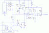
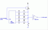
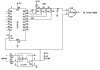
I am trying to take a 4 bit digital signal thru an R2R network and trying to make a varible time delay AC dimmer circuit. What I hope to get is a timed discharge of the cap that will delay a triac gate based on the digital value presented to the R2R resistor network. My problem is that although I understand the digital aspects involved, I have no real clue how to calculate the Resistor or cap values to make an effective dimmer control circuit.. Cab someone take a look at the attached schematic, and help me out. Values do not need to be perfectly linear, I am just trying to control dim incandescent lamps. The circuit is for 120VAC 60 HZ
Thanks
Dialtone
 

Attachments

  • r2r_dimmer_control.jpg
    r2r_dimmer_control.jpg
    47.7 KB · Views: 594
The output of your DAC is constant resistance, variable voltage. This won't work into a TTL gate, which has relatively low gain and a low threshold.
Your simplest solution would actually be to use a microcontroller such as a PIC, but I gather you don't want to do any programming. I could be wrong. :)
Below is a 3 volt ramp generator that should go to zero at each AC zero crossing, and a 4 bit DAC whose output is from zero to about 3 volts. The comparator output goes low when the ramp crosses the threshold. R8 provides hysteresis to assure clean switching. The other half of the LM393 inverts the signal, yielding a rising edge when the delay times out.
I haven't tested or simulated this, so you may have to tweak some values. R5 changes the scaling of the DAC, and R7 changes the slope of the ramp. If the triac gate requires more than 5ma, you will have to add an NPN emitter follower and a couple of resistors at the output. The LM393 can't reliably drive much less than 1k to +5V.
This may be overly complex. I suspect there is an elegant solution (other than the PIC), but I couldn't think of one.
 

Attachments

  • triac_delay.gif
    triac_delay.gif
    10.6 KB · Views: 578
Here is a more detailed explanation of what I thought SHOULD happen. Correct me if I am wrong
1. Normal Idle state (diring the zero crossing interval). Data register outputs are tri-stated, cap is charged high, and fed to NOR gate. Second NOR gate input is also high (from zero cross detector, so output to triac (or opto-coupler-driver) is turned off.
2. After zero crossing, zero cross output goes low gating out data register bits which, depending on their state, drain the cap to a point where the NOR gate input is active low which when coupled with the zero cros detector output low, allows the NOR gate to change output state to drive the triac for the remainder of the current AC half cycle.
3. As the next zero cross nears, the zero cross detector output goes high, which shuts off the NOR gate output, allowing the triac to shut down at zero crossing.

Originally, I intended for the R2R DAC output to be fed to a schmitt trigger (74xx14) and then to a NOR gate, but I posted the schematic in a functional form for simplicity of understanding, instead of the actual components to be used.
Does this make more sense, and can this variable timing trigger delay be
done with off the shelf components and still be kept relatively simple?

Thanks
Dialtone
 
First, the pullup to +5V needs to be 2R if you want all your steps tp be the same size.
Below is a plot of all possible waveforms out of your R-2R ladder (DAC) with R=100k and a 100nF cap on the output. Note that the longest delay is at one LSB, where you have a very slow ramp, and your Schmitt threshold (which is fixed) needs to be about 4.9V in order to get maximum delay. A shallow slope will be very susceptible to noise and temperature fluctuations. A much better solution is a fixed slope ramp and a variable threshold, as in my schematic. You could still use an R-2R ladder instead of the binary weighted one that I proposed, if you like.
A CMOS register will give much more stable and predictable output levels, because the outputs switch rail to rail.
 

Attachments

  • triac_dly_eye.gif
    triac_dly_eye.gif
    9.7 KB · Views: 529
Thanks for the replies Ron. The graph looks good but I do not think the values plotted will do. I need to generate a gate delay who's leading edge(s) fall below a typical schmitt (74HCT14 low detection level of .9v) spaced out over the 8ms interval. Again, the exact intervals do not need to be perfect, just functional enough to get a reasonable facsimile of a dimmer for incandescent lamps. Would be interested to know how you plotted this so I can do the same and substitute different values and see how the plot changes.
Thanks
Dialtone
 
I'm not sure I can describe how I did that graph such that anyone else would understand it. I used Linear Technology's SwitcherCAD III for simulation, and I displayed an eye diagram of the resulting waveform.
That reminds me - with your current schematic, the cap will not be recharged rapidly at zero crossing. You need a switch (transistor) from the cap to +5V to accomplish that.
The schematic below is a variable resistance discharging circuit with a zero crossing reset (the NPN emitter follower). The final voltage for any code should be below the threshold of the Schmitt trigger. You can replace each diode with a base resistor and an NPN common emitter switch if you want lower final voltages. Or, if you can find a quad open drain buffer/gate, that would work.
You should probably make the pullup on your zero crossing detector a lot lower value - like 10k or so. Otherwise, capacitance on the node may not allow the pulse to reach full amplitude.
I still like the constant slope ramp/variable threshold voltage scheme better, but I understand your motivation, and this should work. Let me know if you need help with component selection.
 

Attachments

  • triac_dly_alt.gif
    triac_dly_alt.gif
    5.7 KB · Views: 513
Thanks Ron
Now this a schematic I understand. I wondered if the the cap recharge time was enough in the original schematic, so now I know. I realized, shortly after I posted the schematic, that I made a typing error on the zero cross output resistor value. It should have been 10K and not 210K. Guess I just fat fingered the keyboard

Thanks Again
Dialtone
 
The basic equation for time is resistance * capacitance. For the frequency, do 1 / time.
 
mstechca said:
The basic equation for time is resistance * capacitance. For the frequency, do 1 / time.

How does this relate to his problem? :?: :?: :?:
 
Status
Not open for further replies.

New Articles From Microcontroller Tips

Back
Top