Continue to Site

Welcome to our site!

Electro Tech is an online community (with over 170,000 members) who enjoy talking about and building electronic circuits, projects and gadgets. To participate you need to register. Registration is free. Click here to register now.

  • Welcome to our site! Electro Tech is an online community (with over 170,000 members) who enjoy talking about and building electronic circuits, projects and gadgets. To participate you need to register. Registration is free. Click here to register now.

My final Project

Status
Not open for further replies.

Azziz

New Member
Hi guys
Its my first post in here .
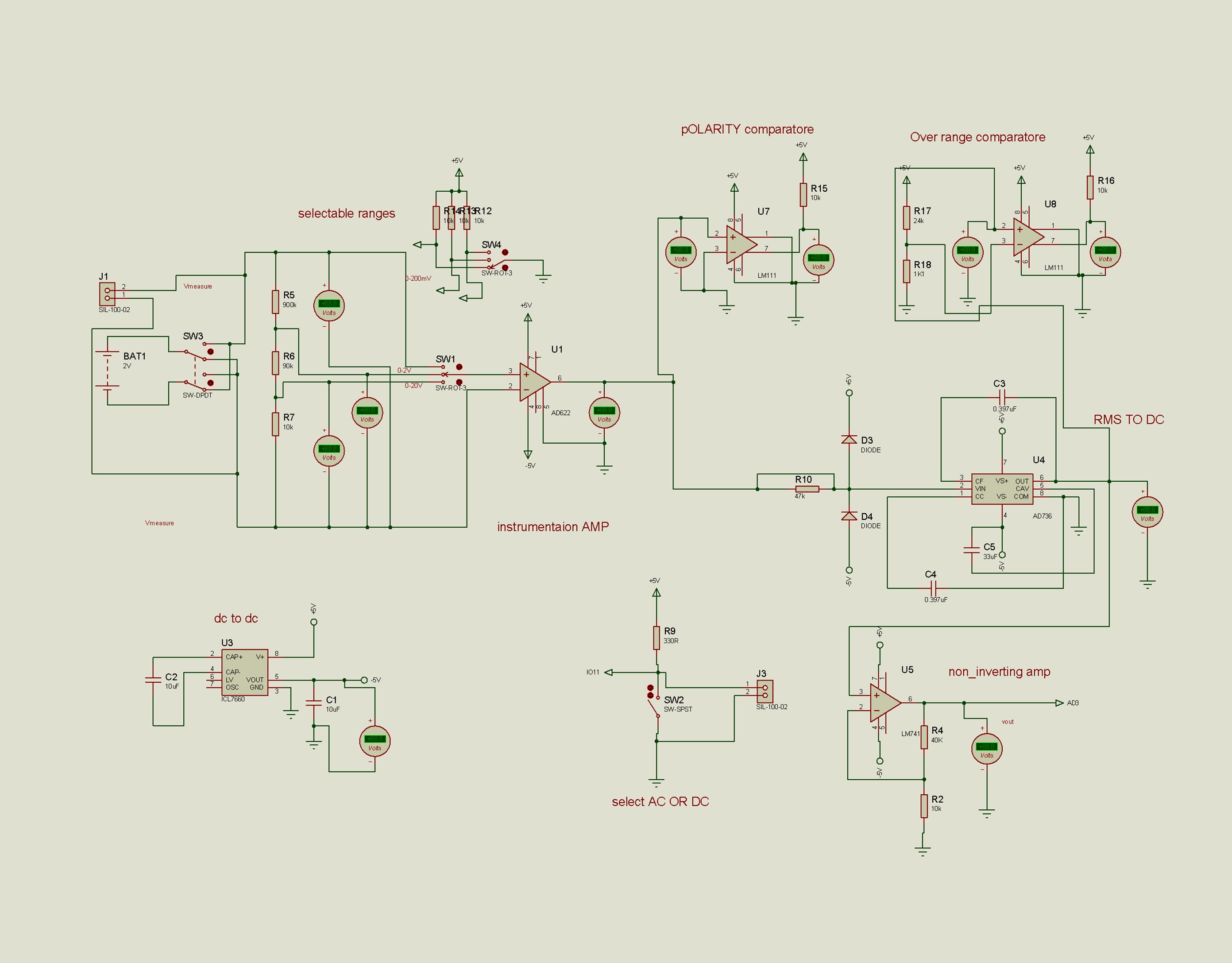
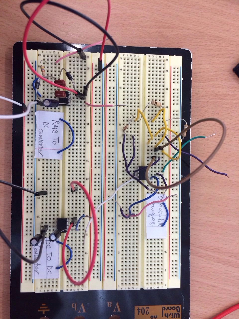
Im currently 3rd years electronic and Im doing my final project this year which is digital voltmeter . Im made the design in isis . after I built the circuit , every component works individually but after putting everything together its not working at all . #
here is the circuit and the design .a friend told me that the problem is the LM311 as a comparator I hope some one can help .
Picture2.jpg
image1.JPG
 
"It' broke" isn't enough information. You should be able to check the ranging, AC-DC converter and the buffer independent of the circuits using the LM311.

I would agree that your friend is right, there is a problem with the LM311 circuit. The LM311 has an open collector output, so it can only sink current. The LED has to go to +V through a resistor and the output will sink to ground or be an open circuit.

I also see at least 4 wires that don't connect to anything on the breadboard. Be sure you know how the breadboard works. In SOME breadboards, the long busses, such s the two on the left are 4 unconnected strips, not two.
 
You have all the simulated voltages for every node. Which ones are wrong? Start with V+/V- and try to add decoupling caps across each chip since you have no ground plane and long wires , to avoid spurious oscillations. All differential OA devices must be 0V for the output to be linear and if + input is greater than (-) the output is high for both comparators and OA's. Otherwise it is dead.

Beware of safe ESD practises.
When you get it working a good idea is to add a common mode choke on the input leads inside to suppress RF and stray AC e-fields and have some kind of over voltage protection and never directly input the chip.

In fact duplicate R10 D3/D4 to both inputs. It serves no purpose between chips of the voltage and remove jumper.

BTW you should tidy up your schematic with short paths and smaller gaps and follow the same practice on the breadboard, keeping the leads flat on the board with the correct solid gauge hookup wire. Long leads tend to act as antenna to cell phone broadcasts which might induce some AM demodulated as DC or noise pulses . When phone is idle , it broadcasts every few minutes to check closest tower signals to receive calls.

SW3 must be integrated with J2 for break before make.
 
Last edited:
YOU NEED TO CONNECT Pin 4 (Vee) on the LM111 to -5V instead of gnd. Split supply is avail, why not use it. Gnd on Pin 1 looks like a differential output on your schematic, when it is not. The output is OC to Gnd.
 
There's another possible issue where there is no place for Ib to drop across. This could explain that each section works independently, but I don;t think the LM311 circuits do.
 
LM111 cannot work if the common mode range is within 1.2~2V of Vee. If the negative rail is ground, then it cannot sense any differential near ground. Hence Vee must be < -2V
 
Status
Not open for further replies.

Latest threads

New Articles From Microcontroller Tips

Back
Top