Continue to Site

Welcome to our site!

Electro Tech is an online community (with over 170,000 members) who enjoy talking about and building electronic circuits, projects and gadgets. To participate you need to register. Registration is free. Click here to register now.

  • Welcome to our site! Electro Tech is an online community (with over 170,000 members) who enjoy talking about and building electronic circuits, projects and gadgets. To participate you need to register. Registration is free. Click here to register now.

MOSFET Driver failures

Status
Not open for further replies.

Mosaic

Well-Known Member
Hi all:
I have a hi energy (1Khz) pulse circuit design. A bank of 4 IRFP3306 NFETS driven by an MCP1407 FET driver that is fed by an optoisolated pulse.
Have a look at the schematic Pic. The switching discharges a low ESR capacitor Bank. Up to 700A peak over a few dozen microsecs.

The MCP1407 output passes thru a 500mA ferrite bead and then splits into 4, 5 ohm gate drive resistors. I note the ferrite bead has a 30C delta temp at peak DC% of 50%.

I have had about 8 driver failures over the last year. The initial failures were quick, after an hour or so, which resulted in adding the ferrite bead, an 18V clamping zener on the FETdriver output and additional decoupling caps. Things seemed ok afterward.

Now, after about 600 hours of runtime, cumulative over about 6 months the FETdriver pops again. The driver input signal switched by the 2n3906 is 12V Hi. Failure mode is the FET driver input pulldown 150ohm (collector resistor load on the 2n3906 transistor) no longer pulls to ground, only to about 5V. There seems to be something preventing the FETdriver input from being pulled low. This causes the FETdriver output to lock hi, overdriving the output FET bank. Simply swapping in a new MCP1407 FETdriver restores normal function.

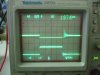
Also, I noted just before the 'failure' of the FETdriver that I started seeing/hearing erratic output pulses, as though signal pulses were either being missed or lasted too long. The pulses are audible (capacitive piezo effect) and abnormal behaviour is easily heard and viewed on a 'scope.

I was looking for some suggestions as to how to rectify this reliability issue. The operating temp of the circuit is around 50C peak (30C ambient).

For now I am planning to change out the gate drive resistors to 10 ohm rather than 5 ohm to relieve some of the loading on the FETdriver and further inhibit ringing. Of course, with a 600 hour test ahead of me, getting it wrong is costly in being unable to get past this. BTW I have a small heatsink on the MCP1407 as a precaution. It runs warm to touch.
FETdrive.png
 
Well, I guess no one has a comment.
I developed a LTspice sim for a method to mitigate the effect of the MOSFET drive failing hi and over-driving the NFET bank.
Basically a soft off with a time constant of about 1 millisec which works out a 100% DC for a 1Khz pulse train.

I share it here for any suggestions or improvements.
 

Attachments

  • MOsfET TOTEm DRIVE&soft_off.asc
    3 KB · Views: 278
I see a note saying there is .1 ohms in the source of the NFETs. It looks like the grounds for the driver and the 150 ohm are connected there. Is that correct?
 
yes..it's a current sense, for the system logic to handle.
That's why I used the optoisolator as the grounds (digital & analog) are different. The MCP1407 and the NFET bank are driven by a different ground (offset by up to a volt (10A curr sense) ).
The main supply passes thru a heavy schottky rectifier, a TVS diode to ground, then 110 uH of hi amp inductors and then charge the cap. bank. The cap bank delivers its pulse via the NFET bank driven by the MCP1407.
 
Last edited:
Have a look at R43 and R48. It would seem to me you would want the 150 ohm driving the base and the 1K as the pull up. Could be the output of the 3906 is in la la land.
 
After rereading the Spec sheet of the MCP1407 driver very closely....I observe that 'some' short duration switching shoot through does happen, which adds to the heating and stress on the part.
**broken link removed**
Section 4.5.3

Page 15 of this doc:
**broken link removed**
Discusses separating the push/pull driver output to eliminate shoot thru.

I think that perhaps adding a 5 ohm resistor between the push/pull outputs should severely limit possible shoot thru to a max of 12V/5 = 2.4A, well below the 6A switching capacity.

Also, on the matter of the gate drive resistors. While 5 ohms seems fine for one or 2 MOSFETS , a bank of 4 in parallel => 1.25 ohms @12V...or possible 12/1.25 = 9.6A peak, (missed that one :banghead:). That exceeds the 6A peak rating of the MCP1407. Moving to 10ohms => 12/2.5 = 4.8A peak which is ok.

There are other factors mitigating peak gate current spike though...trace inductance and the ferrite bead. A differential probe shows a peak of 6V across a 5 Ohm gate resistor for 1.2A per NFET for 5A total peak draw
 
Have a look at R43 and R48. It would seem to me you would want the 150 ohm driving the base and the 1K as the pull up. Could be the output of the 3906 is in la la land.

I guess making them both 1K should be a better design. It's possible that was a mistake...over a year ago now , so I can't recall why a 150 ohm was selected. But that shouldn't zap the driver chip.
 
Yes, should still be ok with the low value. Why not just make the gate resistors 12 ohms then you could be sure. The FET has NC of only 120 so it should still switch fast. Do you see much ringing?
 
What about the NFETs dv/dt being coupled to the gate by Cdg? You have no negative clamping on the output of the gate driver.
 
The lower pulse is the 12V gate pulse using 10X probes.The upper pulse is the Drain side. There's some minor 2-3 Mhz ringing after the pulse shuts off.
@moffy If I remove the 1n4148, the Zener should clamp -ve going transients to 1 diode drop of ground.

Also there seems to be a possibility of latch up at the input if the high current switching transient pulls down the decoupling caps by > .3V drop.
https://ww1.microchip.com/downloads/en/AppNotes/00763c.pdf

I am adding a 150 ohm emitter resistor on the 2n3906 to cut the MCP1407 input signal to 1/2 Vcc to avoid that likelihood. I did note that the failure mode of the chip involved a 5V 'floor' on the input, which the 150ohm load resistor could not pull down to ground.

Another question. As a failsafe, since the NFETS are never always on, would a 1uF ceramic or film cap inline with the gate drive be an acceptable means to block a DC hi from the driver? The pulses don't exceed 300uSec.
 

Attachments

  • 9A mainPulse vs gate.JPG
    9A mainPulse vs gate.JPG
    1.9 MB · Views: 421
Last edited:
It wouldn't hurt to remove the 1N4148, but my statement previously, after some thought, is a bit of nonsense. The -ve dv/dt will be when FET switches on, which means it would have to turn the FET off first before going -ve. It's a self regulating condition. The fact that it takes 6 months to fail sounds more like degrading slowly, due to too much power. Voltage overloads tend to be fast and catastrophic, but that is just a generalisation.
 
I don't think clamping -ve going transients is moot. Hi energy ringing on the drain can couple via the Cdg parasitical capacitiance and possibly pull the MCP1407 output below ground. The application had significant (pulse off) ringing due to the inductance of the load (2-4 uH) to the point of avalanching the NFET output bank at around 70Volts kickback, post pulse. I had 'blown' a few transistors (dead short) due to heating after some hours of service. Since adding a 50SQ series hi pulse schottky in series with a 1uf film cap across the drain/source, the kickback is in the 45V range, below the 60V Vds rating of the NFETS. The NFETS are holding up fine now , even with a 700A switched pulse.

EDIT: I had initially used several 15KE series TVS diodes to clamp the kickback at around 50V. They worked for a few minutes, then physically popped one by one.
 
Yeah, but the failure due to overvoltage was fast and catastrophic not slow and gradual. But you could try a fast schottky in parallel with the zener, it will clamp quickly.
 
Well...As per this app note:
https://ww1.microchip.com/downloads/en/AppNotes/00763c.pdf
I replaced the zener with 1n4148 steering diodes for both Vcc & device ground bounce limiting.
Improved the driver output trace routing to mirror the return path on the double sided board to reduce inductance.
Included two 1 ohm resistors inline with the push pull outputs (thus adding 2 ohms to limit shoot thru currents). This also increases the net gate resistor to 1.25 +1+ .35 + .05 ohms = 2.65 ohms, thus max drive current = 12V/2.65 =4.5A.
Added additional supply decoupling and a ferrite bead on the input. There is a bit of overshoot ringing.
Biased the 4n25 phototransistor base and the inverting 2n3906 base to reduce saturation and improve switching...Now getting sub 8uSec pulse switching with around 4-500ns rise/fall at the 4 power NFET gates.
Placed DC blocking ceramic caps inline with MCP1407 output to add a failsafe to prevent Power NFET switching if the driver fails with a hi output (as it always seems to do) .
Ran a thermographic scan after 10 mins of pulsing and the delta temp on the MCP1407 is under 2 C.


Hopefully there won't be any more failures.
 
Status
Not open for further replies.

New Articles From Microcontroller Tips

Back
Top