Continue to Site

Welcome to our site!

Electro Tech is an online community (with over 170,000 members) who enjoy talking about and building electronic circuits, projects and gadgets. To participate you need to register. Registration is free. Click here to register now.

  • Welcome to our site! Electro Tech is an online community (with over 170,000 members) who enjoy talking about and building electronic circuits, projects and gadgets. To participate you need to register. Registration is free. Click here to register now.

LTSpice simulation - unexpected values

Status
Not open for further replies.

DerStrom8

Super Moderator
Hi all,

First of all I'm going to mention that I very rarely use LTSpice. Usually I use Multisim or Proteus.

I have the following project that was handed to me by another engineer at work. He was having trouble with it so he wanted me to give it a try.
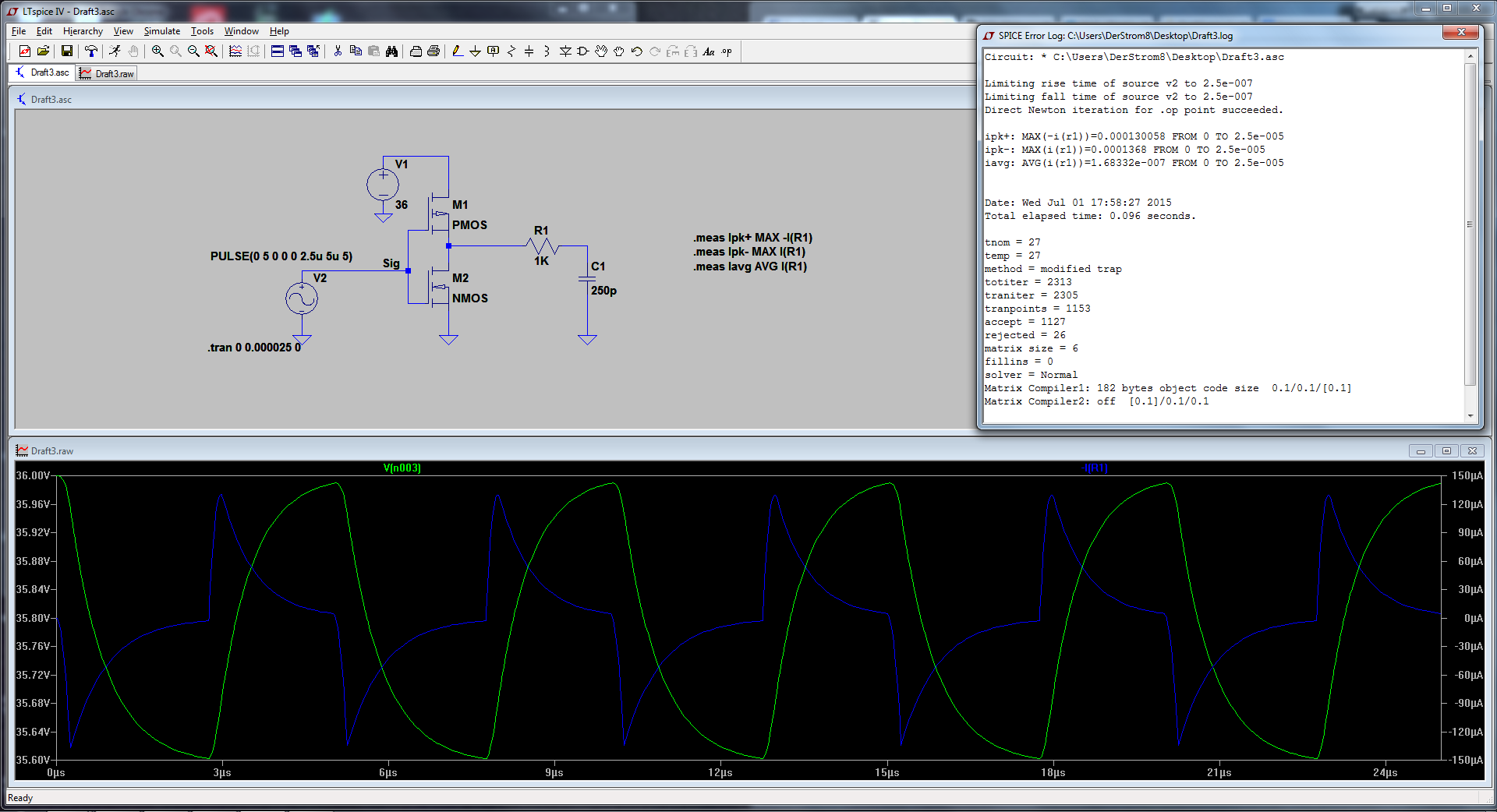
upload_2015-7-1_18-1-15.png


(I am attaching the .asc file as well, for those of you who have LTSpice installed)

I am uncertain about the values I'm getting for Ipk (both + and -). I would expect Iavg to be close to zero (which it is).

Effectively I need to determine the peak current through R1 and calculate the power being dissipated by it so that we can decide which size to use in the new board design. I can't really go into detail on what it is, but you'll have to trust me that the circuit is correct.

V1 is a 36V DC power supply.
V2 is a 200kHz square wave with a 5V amplitude. I do not have any information about the rise/fall times, so I am assuming a perfect square wave.

The two MOSFETs are representing the output stage of a Microchip HV574 (**broken link removed**). I have left out the freewheel diodes.

Can anyone spot any mistakes? The values I'm looking for are:

Ipk(+)(R1)
Ipk(-)(R1)
Iavg(R1)
P(r1)

Thanks folks!
Matt
 

Attachments

  • Draft3.asc
    1.1 KB · Views: 326
The voltage the input is referenced should be 5V (VDD), not the 36V you have shown. With your circuit, the top P-FET will always be strongly on.

If you just want to emulate the output driving the RC, then change the input pulse voltage to swing between 0 and 36V (or just omit the FETs and use a 0/36V pulse as the driver).
Once again the FETs are not discrete, they are the output stage of the HV574. The 5V source may be my issue. I'm not sure how the output stage is driven. I do know that there is 36V on the drain of M1 (the P-MOSFET).
 
I do know that there is 36V on the drain of M1 (the P-MOSFET).
Not at the input stage there isn't. Have a look at the datasheet (excerpt below). VDD is 5V, VPP can be more.
upload_2015-7-2_9-21-33.png
 
Not at the input stage there isn't. Have a look at the datasheet (excerpt below). VDD is 5V, VPP can be more.
View attachment 93147

Ahh, I was looking at the wrong one. The 36V is indeed for VPP. I guess the question now is, how are the high voltage output FETs driven? I see one XOR gate going in, but the FETs appear to have separate gates (according to the HV output stage diagram):

upload_2015-7-1_19-23-19.png
 
I guess the question now is, how are the high voltage output FETs driven?
They'll be driven with a separate driver for the high-side and low-side FETs. The gate voltage of each might only swing 5V to turn each on (they couldn't handle the full VPP across the gate). You don't actually need to know this if you just want to find the current and power in R1 (I addressed this in my first post).
 
They'll be driven with a separate driver for the high-side and low-side FETs. The gate voltage of each might only swing 5V to turn each on (they couldn't handle the full VPP across the gate). You don't actually need to know this if you just want to find the current and power in R1 (I addressed this in my first post).

I must admit, I'm a bit embarrassed about this. I knew they were high-side/low-side FETs and would require separate drivers, but my mind just went the opposite direction :p

If you just want to emulate the output driving the RC, then change the input pulse voltage to swing between 0 and 36V (or just omit the FETs and use a 0/36V pulse as the driver).

I'm just going to feed the 0-36V pulse straight through the RC circuit. Seems to be the simplest way to do it.

Thanks,
Matt
 
M1 is connected upside down; the source should be connected to +36V, not the drain. As it is, it's simply conducting through the substrate diode, which is why you're getting that flakey voltage on your output.

Also, M1 needs its own drive circuit with appropriate voltage levels (+36V and +31V relative to ground).

Once again, I did not design this circuit. It is the output stage of the HV574. It is not connected upside-down (unless, of course, the datasheet is wrong)
 
No, the datasheet shows the correct connection. Look closely at how the P-channel FET's source is connected to Vpp. Your co-worker has the drain going to Vpp instead.
 
No, the datasheet shows the correct connection. Look closely at how the P-channel FET's source is connected to Vpp. Your co-worker has the drain going to Vpp instead.

Wow, I don't know how I missed that! No wonder he couldn't figure it out! :p

Sorry if that previous post came across as rude. That was not my intent :)
 
Wow, I don't know how I missed that! No wonder he couldn't figure it out! :p
Actually, I think the fault lies with the nice folks who created the MOSFET symbol; it comes awfully close to being ambiguous, and I've made that same mistake myself many times.

Sorry if that previous post came across as rude. That was not my intent :)
Not to worry; it didn't!
 
I don't know whether the same is true for Multisim and Proteus, but for LTspice the PMOS symbol and the PNP symbol, by default, are annoyingly 'upside-down' when selected :banghead:.
 
I don't know whether the same is true for Multisim and Proteus, but for LTspice the PMOS symbol and the PNP symbol, by default, are annoyingly 'upside-down' when selected :banghead:.
Yes, they are. (Edit: As most of the time you want them with their source/emitter on top and the gate/base on the left).
I solved that by editing the symbols (located in the sym lib) for those two devices to change their orientation (by rotation and reflection) and then saved them as PNP_INV and PMOS_INV.
Now I can select either orientation, as desired.
 
Last edited:
Actually, I think the fault lies with the nice folks who created the MOSFET symbol; it comes awfully close to being ambiguous, and I've made that same mistake myself many times.
The other extreme annoyance to me is that they chose to use the word saturation to mean something quite different for FETs as compared to BJTs. That seems to be borderline sadistic (how many engineers can we cause to misuse the term). ;)
 
The other extreme annoyance to me is that they chose to use the word saturation to mean something quite different for FETs as compared to BJTs. That seems to be borderline sadistic (how many engineers can we cause to misuse the term). ;)
Ha! I'd forgotten about that one. You're right, it's sadistic!
 
I solved that by editing the symbols
Methinks I'll borrow that idea! Thanks crutschow. I've done some symbol editing in the past; mainly to add a model file to the attributes to avoid having to add a ".inc xxxx.sub" command to each schematic using the symbol.
 
Hi all,

First of all I'm going to mention that I very rarely use LTSpice. Usually I use Multisim or Proteus.

I have the following project that was handed to me by another engineer at work. He was having trouble with it so he wanted me to give it a try.

View attachment 93145

(I am attaching the .asc file as well, for those of you who have LTSpice installed)

I am uncertain about the values I'm getting for Ipk (both + and -). I would expect Iavg to be close to zero (which it is).

Effectively I need to determine the peak current through R1 and calculate the power being dissipated by it so that we can decide which size to use in the new board design. I can't really go into detail on what it is, but you'll have to trust me that the circuit is correct.

V1 is a 36V DC power supply.
V2 is a 200kHz square wave with a 5V amplitude. I do not have any information about the rise/fall times, so I am assuming a perfect square wave.

The two MOSFETs are representing the output stage of a Microchip HV574 (**broken link removed**). I have left out the freewheel diodes.

Can anyone spot any mistakes? The values I'm looking for are:

Ipk(+)(R1)
Ipk(-)(R1)
Iavg(R1)
P(r1)

Thanks folks!
Matt

Hi there Matt,

The RC network is being driven by a square wave, almost exactly.
If the square wave upper voltage is E, then the average power dissipated in the resistor is:

Pavg=(C*E^2*(e^a)-1))/(2*T*(e^a+1))

where
a=T/(R*C), and
T=time of half the cycle of the square wave (cap is either charging or discharging).

Where does this formula come from, and isnt it too simple?
First find the time domain charge equation, then the discharge equation, then combining them to use the final value of the previous mode as the initial value of the next mode recursively, then find the series representation of that result. This provides us with the upper and lower peaks in a closed form.
After that, use the lower peak as the initial cap voltage and time T to calculate the charge voltage expression from the dip to the peak, calculate the expression for the voltage across the resistor from that.
Using that, square it and divide by R to get the instantaneous power, then integrate that over T and divide by T to get the average power in the resistor for that charge cycle.
We could not stop there if it were not a square wave, but since it is a square wave the average power in the resistor is the same for the charge as the discharge, so if we average over T the half period, we get the total average power over the full period 2*T.

The equation could be called beautiful, and that is the beauty of theory.
It would have shown up nice in Latex, but Latex seems to be broken again.
 

Attachments

  • PowerResistorCapChargeDischargeWithSquareWave-1.gif
    PowerResistorCapChargeDischargeWithSquareWave-1.gif
    7.8 KB · Views: 319
Status
Not open for further replies.

New Articles From Microcontroller Tips

Back
Top