Hi,
I'm trying to design/build a custom keyboard but I'm a complete beginner regarding electric curcuits and PCBs.
I followed the PCB-design-tutorial by ai03 (https://wiki.ai03.com/books/pcb-design/chapter/pcb-designer-guide) for a 2x2 macroboard,
tried to expand it and follow the design rules I picked up on various tutorials and videos.
I already checked which pins I'm allowed to use for GPIO and tried to include all necessary files in the attachements.
It would be awesome if one of you could drop some knowledge about potential problems, design flaws, etc and I would love to hear your thoughts on the design.
I do realize that this is a time consuming task so I put together some specific questions:
Additional information:
Thank you!
I'm trying to design/build a custom keyboard but I'm a complete beginner regarding electric curcuits and PCBs.
I followed the PCB-design-tutorial by ai03 (https://wiki.ai03.com/books/pcb-design/chapter/pcb-designer-guide) for a 2x2 macroboard,
tried to expand it and follow the design rules I picked up on various tutorials and videos.
I already checked which pins I'm allowed to use for GPIO and tried to include all necessary files in the attachements.
It would be awesome if one of you could drop some knowledge about potential problems, design flaws, etc and I would love to hear your thoughts on the design.
I do realize that this is a time consuming task so I put together some specific questions:
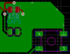
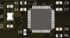
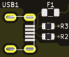
- MCU and Crystal.png: I got told I should place the crystal as close as possible to the Controller. The distance is around 15mm (down from 45mm). Is the difference really that important?
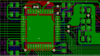
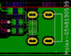
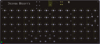
- MCU Zone.png: I got told the same applies to the USB. The distance here is around 30mm (down from 17.5cm). Question is the same as in 1.
- PCB in multiple Layers.pdf/PCB in one Layer.pdf: I only covered parts of the front (GND) and back (+5V) since it's a 2-layer-design. Most PCBs from OpenSource just cover everything in GND on a 2-layer-board. Should I cover one side in GND completely even if everything that's connected to GND is covered by my part-fill?
Additional information:
- 1 & 2: The complete width of the area that can be seen in MCU Zone.png is between 75mm and 80mm.
- 2: I added two pictures of the MCU and Crystal.png using the high contrast mode of KiCAD to better visualize the fill zones. These are called MCU and Crystal Front.png and MCU and Crystal Back.png.
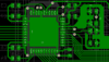
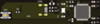
- Unrelated to questions: I added multiple pictures of the boards PCB-design, the schematic and some 3D-visualizations that are not related to the specific questions but the overall topic of a review request. I hope they help. If needed I can add/upload more.
Thank you!
Attachments
-
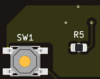
 LED and Button.png42 KB · Views: 381
 -
 MCU and Crystal Back.png141.6 KB · Views: 369
 -
 MCU and Crystal Front.png142.6 KB · Views: 363
 -
 MCU and Crystal.png132.8 KB · Views: 345
 -
 MCU Zone.png71.5 KB · Views: 370
 -
PCB in multiplye Layers.pdf162.3 KB · Views: 362
-
PCB in one Layer.pdf136.2 KB · Views: 375
-
 USB.png67.9 KB · Views: 364
 -
Schematic.pdf254.3 KB · Views: 375
-
 3D Bottom.png136.1 KB · Views: 361
 -
 3D LED and Button.png33.2 KB · Views: 357
 -
 3D LED Top.png19.6 KB · Views: 356
 -
 3D MCU and Crystal.png90.2 KB · Views: 360
 -
 3D MCU Zone Bottom.png51 KB · Views: 369
 -
 3D MCU Zone Top.png27.6 KB · Views: 363
 -
 3D Top.png99.4 KB · Views: 378
 -
 3D USB.png31.6 KB · Views: 370
