Hy all,
The other day I was doing a design which included an LM555 and LMC555 powered from a 12V supply.
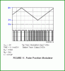
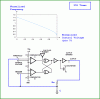
I would have liked to have pulled the 'Control' pin down to 3.33V to alter the comparator references to 3.33V and 3.33V/2, but I could find nothing in the data sheet that defines the use of the Control pin or the voltage limits.
Does anyone have any information/experience in this area?
spec
The other day I was doing a design which included an LM555 and LMC555 powered from a 12V supply.
I would have liked to have pulled the 'Control' pin down to 3.33V to alter the comparator references to 3.33V and 3.33V/2, but I could find nothing in the data sheet that defines the use of the Control pin or the voltage limits.
Does anyone have any information/experience in this area?
spec
")