Continue to Site

Welcome to our site!

Electro Tech is an online community (with over 170,000 members) who enjoy talking about and building electronic circuits, projects and gadgets. To participate you need to register. Registration is free. Click here to register now.

  • Welcome to our site! Electro Tech is an online community (with over 170,000 members) who enjoy talking about and building electronic circuits, projects and gadgets. To participate you need to register. Registration is free. Click here to register now.

Linear transistor regulator question

Status
Not open for further replies.

diy didi

Member
Good day.
I have a question regarding the attached circuit.
R3 and the zener diode sets the reference voltage. Why is R3 connected to the output of the circuit and not to the input?
 

Attachments

  • 438EB28B-4038-4451-BD46-A333F814BA98.jpeg
    438EB28B-4038-4451-BD46-A333F814BA98.jpeg
    1,012.6 KB · Views: 159
R3 is connected to the output as it's a stabilised voltage, so makes the design more accurate - essentially providing a constant current to the zener. Connecting R3 to the input means that it's voltage input, and thus current, will vary - this causes variations in the zener voltage, and thus variations in the output voltage.
 
Not so sure about R3, sim shown running R3 at 560 ohms, and 100K ohms.

The current thru zener varies due to Q2. Maybe its there to boost a min current ?

1672400583884.png


More testing seems like it allows regulation earlier at lower Vin to regulator. So
a min current gets zener into regulation earlier, hence output V.

Load regulation seems unaffected.

Note I eliminated the short circuit current circuitry, its irrelevant to question.


Regards, Dana.
 
Last edited:
Not so sure about R3, sim shown running R3 at 560 ohms, and 100K ohms.

Not sure about what?, it's a standard regulator circuit and I've already explained it's purpose.

It provides a regulated reference current for the zener, and that voltage on the emitter of the transistor is compared to the voltage on the base from the potential divider.
 
Current thru zener varies.....as stated earlier in post #5 and shown in sim.

Here is load regulation, and Iz changing :

1672406252224.png


Regards, Dana.
 
Last edited:
I eliminated it, no substantial effect other than output goes into
regulation a little earlier with a ramped source at input.
 
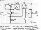
Here is s simplified way to analyze this circuit. Think of TR2 (Q2) as an opamp. The emitter is the non-inverting input, the base is the inverting input, and the emitter of TR1 (Q1) is the output.

With no feedback, the transition voltage at the base is (Vz + Vbe, or 6.2 V with idealized components. This is the same as an opamp with a 6.2 V voltage reference connected to the non-inverting input. With no feedback, the "opamp" acts as an inverting comparator: as the voltage at the base goes above and below this voltage level, the output goes from saturated-low to saturated-high

RV1 and R4 form a negative-feedback voltage divider, just like the feedback resistors around a non-inverting opamp. The gain equation is the same. For example, if R4 and the adjusted value of VR1 both are 1K, the output will be 12.4 V.

Because a real opamp has way more forward gain than one transistor (Q2 is an emitter follower, and provides no voltage gain), the overall voltage regulation will not be as good. Also, because Q1's base current will be greater than a real opamp's input bias current, the calculated output voltage will be slightly off because this bias current is being drawn through one of the gain-setting resistors (VR1).
 
Status
Not open for further replies.

Latest threads

New Articles From Microcontroller Tips

Back
Top