Continue to Site

Welcome to our site!

Electro Tech is an online community (with over 170,000 members) who enjoy talking about and building electronic circuits, projects and gadgets. To participate you need to register. Registration is free. Click here to register now.

  • Welcome to our site! Electro Tech is an online community (with over 170,000 members) who enjoy talking about and building electronic circuits, projects and gadgets. To participate you need to register. Registration is free. Click here to register now.

Keypad with latched switches

Status
Not open for further replies.

malsch

New Member
Hi,

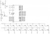
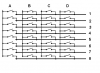
i am using the 8051 and am having trouble with scanning a 2x8 keypad. This is due to the fact that the switches are latched ones (push to make switch). Also more than one switch can be pressed at one time.

The code written, scans each column (the column which is being scanned is set to low) and when a switch is pressed, the output pin is set to low when the column is scanned. The problem arises when more than one switch is pressed in each column. I think this is because when more than one switch is pressed, both the input and the output pins are then set to low due to the two (or more) columns being shorted together. If anyone can help, it would be greatly appreciated. Thank you

Code:

#define Rows P1
#define Columns P2
#define DigitalOP P3

void main(void)
{
while(1)
{
Columns=0xFE;
BPMDelay(1000);
Columns=0xFD;
BPMDelay(1000);
Columns=0xFB;
BPMDelay(1000);
Columns=0xF7;
BPMDelay(1000);

}
}
 

Attachments

  • 111.JPG
    111.JPG
    50.7 KB · Views: 368
Last edited:
The P2 pins should drive the columns via diodes (with pull-up resistors), to prevent a latched switch from holding a P1 pin Hi while a P2 pin is trying to pull it Lo.
 
Shouldn't do... If you have a 0v signal on P1.1 and you have external pullups on P2.. As you will only read P2 on each iteration ie.. P1.0 & P1.1 you then can determine if one or both switches are pressed.
 
thanks for replying. you mean like this:

**broken link removed**

or a single diode for every pin (for P2)?

So the diodes prevent each switch from influencing any of the other pins by blocking the voltage. I am understanding correctly?
 
Shouldn't do... If you have a 0v signal on P1.1 and you have external pullups on P2.. As you will only read P2 on each iteration ie.. P1.0 & P1.1 you then can determine if one or both switches are pressed.

so is there a way to create an 8x8 keypad with latched switches?
 
I'm not clear whether the rows or columns are being used as inputs and whether the columns or rows are being pulsed Hi of Lo in the above schematic but, yes, that's the general idea (although it's obviously more elaborate than you need for your 8 switches).

If you want an 8x8 keypad then it's just an extension of the above schematic to 8 rows and 8 columns.
 
Last edited:
i have applied the diodes in proteus. But the simulation doesn't work. when a low is passed trough the diode, a high is outputted from the diode. i cant understand why. Port 2 and Port 1 both have internal pull-ups so there is no need to apply them.
 

Attachments

  • dgg.jpg
    dgg.jpg
    31.3 KB · Views: 332
I really can't see your problem... if you have P1 (0 through 3) supplying 0v in turn to the keypad rows with internal pullups on P2, when you read P2 this gives you which key is on or off in that column.

P1.0=0, P1.1=1,P1.2=1, P1.3=1
Read P2 (provides column A result)

P1.0=1, P1.1=0,P1.2=1, P1.3=1
Read P2 (provides column B result)

P1.0=1, P1.1=1,P1.2=0, P1.3=1
Read P2 (provides column C result)

P1.0=1, P1.1=1,P1.2=1, P1.3=0
Read P2 (provides column D result)

They won't clash atall.. If in the picture Row B is 0v only those keys are affected
if 1 AND 4 are pressed P2 will read 9 denoting two keys are pressed.

Similarly, If row A is 0v and 1 is pressed AND row C is 5v and 1 s pressed, P2 will read 1 on the A scan and then 1 when the C row is scanned.
 

Attachments

  • keypad.png
    keypad.png
    13.9 KB · Views: 342
@malsh
Your diodes are the wrong way round if you are taking P2 pins low in turn and reading P1 (as your code implies). But they are the right way round if you were to take P1.0 and P1.1 low in turn and read P1 instead (needing modified coding).
The present coding arrangement of writing to P2 and reading P1 needs 8 writes and 2 reads. It would be more code efficient (2 writes and 2 reads) to write to P1 and read P2.

@Ian
The problem with not using isolating diodes is this. Suppose in your post #8 circuit you have row 1 Lo while rows 2-8 are Hi. If now the top switch and another switch in column A are closed at the same time, row 1 (Lo) will be shorted to another row (Hi). The result will, at worst, be damage to the micro and, at best, be an indeterminate logic level to be read at column A.
 
Last edited:
Think of the row as a memory address and the switch wire-or's the binary value. The OR is made through the row index and the switched diode.
 
You can do it without diodes by setting only the pin you are taking low to output and the rest to input. You will still get a "ghost" keydown if 3 corners of a square are pressed simultaneously (the forth corner appears to be pressed as well due to a path being made through the 3 pushbuttons).

Mike.
 
I agree with Pommie... If you use tri-stated pins you wouldn't need extra circuitry, If column A button 1 AND column B button 1 were both on then a short wouldn't happen and both switches could be read correctly.
 
how do you set them as inputs and outputs? but if you have a "square corner" pressed, you would still have the ghost key problem im guessing. by the way, what are tri-stated pins? is it when they are set to input or output?

Thanks again :)
 
Tri-stated means that the pin is high impedance and not actively low or high. The way to achieve this on a microcontroller is to set the pin to input. However, some 8051 variants have open collector outputs and so can be tri-stated by making them high.

Mike.
 
Status
Not open for further replies.

Latest threads

New Articles From Microcontroller Tips

Back
Top