Continue to Site

Welcome to our site!

Electro Tech is an online community (with over 170,000 members) who enjoy talking about and building electronic circuits, projects and gadgets. To participate you need to register. Registration is free. Click here to register now.

  • Welcome to our site! Electro Tech is an online community (with over 170,000 members) who enjoy talking about and building electronic circuits, projects and gadgets. To participate you need to register. Registration is free. Click here to register now.

Is my schematic fine?

Status
Not open for further replies.

Sashvat

Member
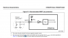
Hi guys, I am making a Microcontroller board for myself, I am using a STM32F103C8T6 ARM cortex M3 processor. I checked the data sheet and made this schematic and would want to know if everything is fine and good to use as a Microcontroller development board. If there is any mistake I have made please let me know.

Thank you.
 

Attachments

  • Schematic_STM32F103C8T6-MC-board_Sheet-1_20190602100246.pdf
    52.6 KB · Views: 218
How does C14 get charged?

Mike.

The MCU has an integrated pull up resistor and gets charged by that. You can check this screenshot I have taken from the data sheet, I just followed what the data sheet says
 

Attachments

  • Screenshot 2019-06-03 at 12.56.42 PM.png
    Screenshot 2019-06-03 at 12.56.42 PM.png
    137.4 KB · Views: 201
That was the only thing I found questionable except for the schematic being upside down - Gnd is normally down.

Mike.
 
How do you program the thing? There's no programming header
 
How do you program the thing? There's no programming header

I have updated it and added one also in my schematic, also I though I could connect the SWDIO and SWCLK pins by placing a pad on my PCB and connecting them directly to the pins on the Microcontroller would that be fine?
 
So guys, this is my updated schematic, I have added LED's to my board and a connector to program it, LED 1 is for power and LED 2 is for PC13. Let me know if this is fine.
 

Attachments

  • Schematic_STM32F103C8T6-MC-board_Sheet-1_20190605093135.pdf
    55.1 KB · Views: 218
I thought the symbol was fine not the orientation
The orientation is important.

A schematic tells a story, and needs organization to make the information flow more easily to the viewer. There are standards for symbols, and "rules of the road" for industry common practices. The more you conform to these, the easier it is for a stranger who knows nothing about you or your design to "get" what it is you are trying to achieve. Also, the schematic is *the* reference document for a design or project. It needs to capture everything that might be important down the road for purchasing and manufacturing. Of course, much of this doesn't necessarily apply to a one-off home project, but there is no good reason for an amateur not to adopt the practices of a pro when appropriate.

Grounds always point down.

Power flows from top to bottom. Positive voltage sources toward the top or upward pointing, negative sources toward the bottom or downward pointing. For a decoupling capacitor on a negative rail, ground symbol is above but downward pointing, negative voltage designator is below and downward pointing.

Signals and power flow from left to right.

Unique reference designators for every component.

Pin headers, plugs, and male connectors start with P. Sockets of all types start with J. Some companies have internal rules that dictate P or J for all connecting devices, but I've found that this can lead to gender errors on the BOM.

Always put mounting holes (and SMT fiducials) on the sch as components. They sometimes have electrical connections, and it forces you to include them in the earliest stages of the pc board layout.

Paper and electrons are cheap. Spread things out to prevent crowding, as in the C12 / C9 area, and unnecessary crossed line like the net to C14.

A schematic is a *design* document, not a production wiring diagram. There is no reason to keep datasheet pinout orders. Re-arrange the pins to make the signal flow more clear. (In my schematic library I have six different decals for a 555.) U1 is neither, because the pin arrangement is not like the physical device, yet causes signal congestion.

For a large component like U1, I would start by re-arranging the pins so all of the power and GND pins are on the left, down low. All dedicated pins like clocks, reset, and programming on the left, and any I/O ports configured as inputs on the left. I/O ports configured as outputs on the right. If that puts too much stuff on one side, then maybe move some of the power pins to the right. Or keep all housekeeping on the left, and all I/O on the right. Again, there is no hard and fast rule, but moving the pins around can do wonders for clarity, and clarity prevents errors.

Grounds always point down.

ak

Thank you so much for your patience in writing this out. I will correct myself and upload it again thanks a ton! just a small doubt, can you explain me the decoupling caps for my case? because if I keep ground on top, the Polarity changes, do I need to change the position of my pins in U1?

and I have included a male jumper connection to all the GPIO pins from the library and added it to my schematic, would that be good for what you said for pin headers?
 
Last edited:
My vote is that orientation beats crosses. If you are not going to reverse the pins in the U1 decal, then I'd re-orient the capacitors so V+ is up and GND is down, and live with the crossed wires.

The U reference designator is universally used for integrated circuits, and I've never seen it used for connectors. A USB connector is hermaphroditic, so it doesn't automatically get either P or J. Since you are plugging an external cable into it, I'd go with J.

AND, the USB connector is an excellent example of the clarity benefit of rearranging the U1 pinout.

ak
 
The U2 3.3V LDO regulator has no part number. Is only 1uF correct for C13, its output?
What is the input voltage of U2?
 
My vote is that orientation beats crosses. If you are not going to reverse the pins in the U1 decal, then I'd re-orient the capacitors so V+ is up and GND is down, and live with the crossed wires.

The U reference designator is universally used for integrated circuits, and I've never seen it used for connectors. A USB connector is hermaphroditic, so it doesn't automatically get either P or J. Since you are plugging an external cable into it, I'd go with J.

AND, the USB connector is an excellent example of the clarity benefit of rearranging the U1 pinout.

ak

but the caps are all non-polarised, so what I did in my updated schematic (still working on all the points you told me) I rearranged the pins so that VDD is on top and VSS is below it. would that be good?

So a J for USB?
 
If you gather all the decoupling capacitors together then they can be orientated correctly. There position on the schematic is irrelevant - only there position on the board is important.

Mike.
 
Why reinvent the wheel?, you're basically trying to copy the 'blue pill' board, which is available FAR cheaper than you can possibly buy the parts for.

The 'blue pill' also includes a couple of jumpers, for selecting programming or run modes.
 
Why reinvent the wheel?, you're basically trying to copy the 'blue pill' board, which is available FAR cheaper than you can possibly buy the parts for.

The 'blue pill' also includes a couple of jumpers, for selecting programming or run modes.

I just want to learn how to make my circuit get my hands dirty and make them my self. I do have the blue pill, but unable to program it because I have a Mac. Also, there are some chips which suit my needs but aren't in Microcontroller development boards, so for that reason I wanted to learn from somewhere so I started this.
 
Last edited:
Guys I have done my schematic the way you have advised me, please let me know if this would work, thank you all for your patience.

this is a different chip I have used, just FYI.
 

Attachments

  • Schematic_STM32F334K4T6-MCU-development-board_Sheet-1_20190609160312.pdf
    64.2 KB · Views: 186
Last edited:
Status
Not open for further replies.

Latest threads

Back
Top