Hi,
Pic24 seem interesting, but I wonder if it's possible for a hobbyist like me to etch a pcb with such thin tracks .
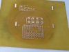
In the datasheet, the pitch is said to be 0.5 mm with 0.2 or 0.3 mm track width.
Has someone succeeded to etch such thin tracks ?
Up to now I've using laser printer and iron perchlorure , but I am ok to try other
technique if it's possible to get thinner tracks.
Thanks,
Cédric
Pic24 seem interesting, but I wonder if it's possible for a hobbyist like me to etch a pcb with such thin tracks .
In the datasheet, the pitch is said to be 0.5 mm with 0.2 or 0.3 mm track width.
Has someone succeeded to etch such thin tracks ?
Up to now I've using laser printer and iron perchlorure , but I am ok to try other
technique if it's possible to get thinner tracks.
Thanks,
Cédric