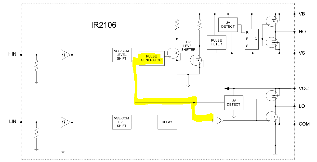
The functional circuit, as per the datasheet, is this :-

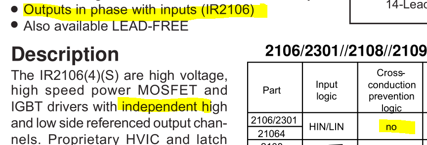
I'm puzzled as to the exact operation of the highlighted section, which seems to show the Hi driver's pulse generator controlling the Lo driver's output via the NOR gate, despite the introductory text saying :-

I could understand a desire to force the LO output low when the HO output is high, to prevent cross-conduction, but the table says that no cross-conduction prevention logic is present.
I also wonder if the NOR gate should really be a NAND gate, in order to force LO low (not high) when the under-voltage detection logic senses too low a Vcc voltage.
Any thoughts?
I'm puzzled as to the exact operation of the highlighted section, which seems to show the Hi driver's pulse generator controlling the Lo driver's output via the NOR gate, despite the introductory text saying :-
I could understand a desire to force the LO output low when the HO output is high, to prevent cross-conduction, but the table says that no cross-conduction prevention logic is present.
I also wonder if the NOR gate should really be a NAND gate, in order to force LO low (not high) when the under-voltage detection logic senses too low a Vcc voltage.
Any thoughts?

