Continue to Site

Welcome to our site!

Electro Tech is an online community (with over 170,000 members) who enjoy talking about and building electronic circuits, projects and gadgets. To participate you need to register. Registration is free. Click here to register now.

  • Welcome to our site! Electro Tech is an online community (with over 170,000 members) who enjoy talking about and building electronic circuits, projects and gadgets. To participate you need to register. Registration is free. Click here to register now.

Ingenious high side transformer isolated gate drive is too good?

Status
Not open for further replies.

Flyback

Well-Known Member
Hello
One of our contractors has just posted us a schematic with a high side transformer isolated FET gate drive design on it, in an offline power supply that he designed
Put it this way, this circuit does not appear in here…..
https://www.tij.co.jp/jp/lit/ml/slua618a/slua618a.pdf
Its extremely ingenious, and yet, rather simple.
What I cannot understand is why I can’t find it anywhere on the web.
If you’ve seen this design youll know the one I mean. It appears to bypass many of the usual problems with transformer isolated gate drives.
Do you know the origin of it?
I am currently on a gremlin hunt of it, because this design is so brilliant that I suspect there must be a gotcha…do you know of any?

He's got a working prototype, and it works well on the simulator at my end.
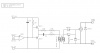
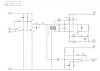
I cant post the schem, but if you know this circuit, then you'll know exactly what i am talking about
 
You've provided no info of this "ingenious" circuit and expect us to be able to comment on it's problems and origin? Why are your posts always like this?
 
Last edited:
All i can tell you is a clue..."flick on, flick off"
I cant say any more.
if you know of it, you will know what i am talking about.
 
I think that's the one - does it look something like this? As Ron suggests, the edges through the transformer are used to turn the FET on and off, and the holding charge is stored in the gate capacitance for as long as it's needed. As you can see, I came up with this idea nearly 7 years ago, so I'd imagine that a few people have come up with it independently over the years.
The disadvantages would seems to be that it's a bit tricky to get working right, and has a substantial holding current (at least, my version does). I knew virtually nothing about magnetics when I played with this - and I'm still no expert - but the trick seems to be that between switching edges the flux must be held constant, or only allowed to change relatively slowly, in order to avoid inducing significant voltage at the secondary side.

I'd be interested to hear others' input on this technique, too. I think I have seen it elsewhere, but only rarely.
 

Attachments

  • snip1.png
    snip1.png
    34 KB · Views: 125
Other disadvantages might be that, because there is no consistent pull-up or -down on the gate, the gate voltage could be susceptible to change though stray leakage, noise, Miller effect, etc - potentially turning the FET on or off when you didn't intend to.

----
I developed the above circuit a bit further, too. This one can automatically shut itself off on an over-current, and flag that it has done so to the controller. I seem to remember that it was quite reliable (but not good enough to save itself when I let it overheat).
 

Attachments

  • snip2.png
    snip2.png
    47.8 KB · Views: 108
If that's the one then that's just been packaged into Analog Device's iCoupler gate drivers ICs. I use those all the time.
 
Could be, but from this paragraph from the datasheet:
"Unlike other optocoupler alternatives, dc correctness is ensured
in the absence of input logic transitions. Two different fail-safe
options are available by which the outputs transition to a predeter-
mined state when the input power supply is not applied."
I think they might be using a carrier-based approach - I believe that's what other digital isolators (like the Silicon Labs Si8640) do.
 
Ah yes, here indeed it is...Ron was onto it i believe
Going to do a gremlin search now.
Figure 7 in the attached.
 

Attachments

  • Large duty cycle Txfmr gate drive.pdf
    37 KB · Views: 108
Floating un-driven gate, could, i reckon, fall victim to noise.
I would be worried about disturbances coming through the CDG capacitance and turning it on or off, because the fet is essentially un-driven.

The lack of popularity of this method suggests some serious ills.

Thouigh when you consider all the ills of other pulse transformer gate drives, this 2_fet_secondary (as in post #10) method seems too good to be true.
It means a much smaller pulse transformer can be used.
Long ON or OFF times are easily catered for.
High duty cycles are no problem whatsoever.
There is no series AC coupling capacitor there, so no LC oscillation with the primary inductance needing damping.
It avoids the problem that some transformer gate drives have where the drive voltage reduces as the duty cycle increases.

So why is this gate drive method not more often used?
 
Many of the ICs have a restriction that the top side transistor must not go below ground.
Many of the ICs require the bottom transistor and the PWM be on the same ground.

With transformer isolation the transistors do not have to be on the same ground as the PWM.

For many decades I designed quiz-resonant power supplies with 1000V, 1200V, 1500V and 2kv transistors. (not MOSFETs)
Many of those transistors only came in a TO3 case. The Collector is the case.
Every one but "us" connected the Emitter to ground and drove the Base. (simple) Problem is the Collector has high voltage on it. (850 to 1350 volts) Usually in the range of 30khz to 120khz. If you touch the collector it will burn the skin off. Very dangerous. You must insulate the transistor from the heat sink. The insulators are pushed to the max and the bolts that hold the transistor must have insulated shoulder washers. There was many problems with these insulators not surviving over time.
We chose to connect the collector to the supply, (75 to 200V) and let the B-E have the pulse on it. So the insulators needs to with stand only 200V. (safe and no more exploded insulators)

Because we understand transformers; I used the "Base Drive Transformer" as insulation.
Simple drawing of "high voltage switch". It is used some thing like a Emitter follower.
1554912163878.png

"Why a capacitor across the transistor?" These HV transistors are slow. The C and L(s) not shown make a LC. The supply is in resonant mode. This reduces the power lost in turn on or off. Allowing very high frequency switching.
 
Status
Not open for further replies.

New Articles From Microcontroller Tips

Back
Top