Continue to Site

Welcome to our site!

Electro Tech is an online community (with over 170,000 members) who enjoy talking about and building electronic circuits, projects and gadgets. To participate you need to register. Registration is free. Click here to register now.

  • Welcome to our site! Electro Tech is an online community (with over 170,000 members) who enjoy talking about and building electronic circuits, projects and gadgets. To participate you need to register. Registration is free. Click here to register now.

identifying the correct point of Ic(sat)

Status
Not open for further replies.

qtommer

Member
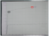
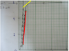
i am doing an experiment on the dc characteristics of the BJT and have drawn the output characteristic curve for values of IB=20uA and IB=50uA (Refer to attachment)

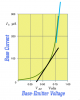
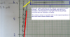
In order to find the beta of the transistor, I take Ic(sat) / Ib.
Referring to the 2 points of the graph i have circled in the attached pic, which point should I take for Ic(sat)? The point where the curve starts to become horizontal [black box] or the point right at the end (highest point of Ic) [red box]?

help is extremely appreciated. thanks=)
 

Attachments

  • Untitled picture.png
    Untitled picture.png
    1.1 MB · Views: 696
Hi,

The area where the black box is located is a better approximation than where
the red box is. The red box shows an area where the transistor has already
been forced out of saturation. The black box shows an area where the transistor
is just starting to be forced out of saturation.

Some oscillators use this principle to oscillate. The collector current starts to
increase more and more and eventually it reaches the point at that black box
where it starts to come out of saturation and so the collector voltage starts
to rise suddenly and that causes another part of the circuit to shut off the transistor
completely, and that's half of the oscillation cycle.
Some of those small LED booster circuits use this principle to boost the voltage
needed to drive a white LED.
 
Last edited:
At the red box the transistor is a linear amplifier with a base current that is very low (its beta defines its collector current/base current).

The black box is where the transistor is almost saturated but its collector-emitter voltage is too high because its base current is too low.

The datasheet shows that a little transistor saturates best when its base current is 1/10th the collector current which is not beta.
 
Last edited:
ahh that clears up alot of confusion in my mind...thank you both so much for your replies...

i have another question. referring to the pic attached of Ib versus Vbe..should i calculate the small signal input resistance by taking the gradient at the black line or the blue line...i have strong feeling its the black line because its is only then where the signals are "small"..is my assumption correct?

Likewise, As for the dynamic output resistance on the output curve, I will take the gradient at the ohmic region of the curve as it is also at the region where the signals are "small"?

thank you
 

Attachments

  • Untitled picture.png
    Untitled picture.png
    357.6 KB · Views: 309
Saturation is where you are trying for lowest Vce voltage.

For a given Ic, it is typically defined at a forced beta of 5 in order to meet a minimum Vce spec.

For example, if a transistor spec'd for Vce sat of 0.05 vdc at 200 mA you will typically see in the spec notes that a base current of 40 mA is applied.
 
Last edited:
i have another question. referring to the pic attached of Ib versus Vbe..should i calculate the small signal input resistance by taking the gradient at the black line or the blue line...i have strong feeling its the black line because its is only then where the signals are "small"..is my assumption correct?
You are looking at the dynamic impedance of a diode. A transistor input impedance is its internal Re plus any external RE times its hfe.
I simply look at the input impedance graph in the datasheet for the 2N3904 transistor.
 
Saturation is where you are trying for lowest Vce voltage.

For a given Ic, it is typically defined at a forced beta of 5 in order to meet a minimum Vce spec.

For example, if a transistor spec'd for Vce sat of 0.05 vdc at 200 mA you will typically see in the spec notes that a base current of 40 mA is applied.
The "forced beta" for the 2N3055 power transistor is 3 (IC=10A).
The "forced beta" for the 2N3904, 2N4401, 2N2222 and BC337 is 10.
The "forced beta" for the BC547 is 20.
 
You are looking at the dynamic impedance of a diode. A transistor input impedance is its internal Re plus any external RE times its hfe.
I simply look at the input impedance graph in the datasheet for the 2N3904 transistor.

assuming that there is no external RE, is it correct to just obtain the impedance by finding delta Vbe/ delta Ib from the input graph
I read that for this purpose, the value of Ib is obtained by setting the value of Ic to a fixed value (say 5mA)
why is this so?


and as for the output resistance..i can evaluate this value graphically by finding delta Vce / delta Ic..
at which part of the graph should i evaluate? the ohmic region or the saturated region? some books evaluate this at the ohmic region but i just read a book which evaluates this at the saturated region...

thanks..
 
assuming that there is no external RE, is it correct to just obtain the impedance by finding delta Vbe/ delta Ib from the input graph
I read that for this purpose, the value of Ib is obtained by setting the value of Ic to a fixed value (say 5mA)
why is this so?
The input impedance of a transistor drops as its current is increased. I think its input impedance is much higher than for a diode.

as for the output resistance..i can evaluate this value graphically by finding delta Vce / delta Ic..
at which part of the graph should i evaluate? the ohmic region or the saturated region? some books evaluate this at the ohmic region but i just read a book which evaluates this at the saturated region...
The output current of a transistor barely increases as its collector voltage is increased. It rise due to the Early Effect. The collector load resistor dominates the output resistance of a transistor circuit.
 
Last edited:
Originally Posted by qtommer View Post
assuming that there is no external RE, is it correct to just obtain the impedance by finding delta Vbe/ delta Ib from the input graph
I read that for this purpose, the value of Ib is obtained by setting the value of Ic to a fixed value (say 5mA)
why is this so?
The input impedance of a transistor drops as its current is increased. I think its input impedance is much higher than for a diode.

I see ... so is 5mA considered a typical value used for analysis?

as for the output resistance..i can evaluate this value graphically by finding delta Vce / delta Ic..
at which part of the graph should i evaluate? the ohmic region or the saturated region? some books evaluate this at the ohmic region but i just read a book which evaluates this at the saturated region...
The output current of a transistor barely increases as its collector voltage is increased. It rise due to the Early Effect. The collector load resistor dominates the output resistance of a transistor circuit.


so the correct method is to analyze the del of vce to the del of the ic on the output characteristics graph at the saturated region?
 
Look at the Input Impedance graph in the datasheet of the 2N3904 transistor. It shows the collector current from 130uA to 10mA and it is a straight line on the logarithmic chart.

The output impedance of a common-emitter transistor is valid only when the transistor is linear, not saturated and not cutoff.
 
i observed the input impedance graph of the 2n3904 and got the corresponding input resistance of 1kohm for Ic=5mA

i calculated the input resistance from my graph and got a value of 1.25k ohms when Ic = 5mA...

however I used the BC108 for this experiment ..As both these input impedance values are almost the same from both transistors,my question is will input resistance values for different types of transistors be approximately similar at the same values of Ic?

I would like to compare my calculated result with a datasheet value to validation purposes but the BC108 datahseet provides no graph whatsover for me to make this validation.

The only data that it provides me is the value of input resistance when Ic = 2mA which is 4.8kohms...

however from this, I can prove that as the value of Ic decreases, the value of the small signal resistance can increase....


As for the dynamic output resistance, there are no values at all for me to validate my calculated answer of Rout=20ohms...

Is there any way I can validate my calculated value of Rout?
 
The input impedance of a common-emitter transistor is its internal emitter resistance times its hfe. All transistors have the same internal emitter resistance (0.026/emitter current) but the 2N3904 has a range of hfe of about 110 to 330 and the BC108 has a much wider range from about 120 to 900. The MPS-A18 transistor has a range of hfe from about 550 to 1600 so it would have a high input impedance. Power transistors have low gain and high current so they would have a very low input resistance.

The output resistance of a common-emitter transistor is its collector resistor because the collector is a high impedance current source. The Early Effect causes a collector to have some measurable resistance.
 
The input impedance of a common-emitter transistor is its internal emitter resistance times its hfe. All transistors have the same internal emitter resistance (0.026/emitter current) but the 2N3904 has a range of hfe of about 110 to 330 and the BC108 has a much wider range from about 120 to 900. The MPS-A18 transistor has a range of hfe from about 550 to 1600 so it would have a high input impedance. Power transistors have low gain and high current so they would have a very low input resistance.


thank you!

referring to
The output resistance of a common-emitter transistor is its collector resistor because the collector is a high impedance current source. The Early Effect causes a collector to have some measurable resistance.

and also:

The output impedance of a common-emitter transistor is valid only when the transistor is linear, not saturated and not cutoff.

Through graphical analysis, I evaluated the change in Vce/Ic to find the output resistance which supposed to be 1kohm (The value of Rc)
[refer to attached pic]

When i evaluated at the point of the yellow gradient, i yielded 200ohms but when i evaluated at the red gradient, i got 20ohms...when i evaluated the gradient across the saturated (horizontal) line, i got 4000 ohms...

which is the correct point that i should evaluate to get the correct output resistance? (1000ohms)

thanks
 

Attachments

  • Untitled picture.png
    Untitled picture.png
    848.5 KB · Views: 229
The collector impedance of a common-emitter transistor is very high.
 

Attachments

  • collector impedance.PNG
    collector impedance.PNG
    648.6 KB · Views: 210
once again thank you so much=)


i have one final question:

after evaluating the gradient at that section i obtained a value of Rout=6432 ohms..

is there any way i can validate this value of Rout theoretically without considering the effect of the collector resistor in parallel....which then reduces the resistance to the value of Rc...?

thank you
 
once again thank you so much=)


i have one final question:

after evaluating the gradient at that section i obtained a value of Rout=6432 ohms..

is there any way i can validate this value of Rout theoretically without considering the effect of the collector resistor in parallel....which then reduces the resistance to the value of Rc...?
On your first graph I calculated that the collector current increased from 5.8mA when the collector voltage was 0.4V to 6.6mA when the collector voltage was 4.4V. Then the collector impedance was 5k ohms.
The collector resistor is about 807 ohms (5V/6.2mA) if the supply is 10V.
 
Hi, you should draw a the graphic of the CE circuit, it is a line starting from total conduction (transistor conducting) to no conduction, the point that the two graphs have in common is the ic(sat).
 
Status
Not open for further replies.

Latest threads

New Articles From Microcontroller Tips

Back
Top