Continue to Site

Welcome to our site!

Electro Tech is an online community (with over 170,000 members) who enjoy talking about and building electronic circuits, projects and gadgets. To participate you need to register. Registration is free. Click here to register now.

  • Welcome to our site! Electro Tech is an online community (with over 170,000 members) who enjoy talking about and building electronic circuits, projects and gadgets. To participate you need to register. Registration is free. Click here to register now.

How/Where To Add Circuit Protection DC/DC Buck Converter?

Status
Not open for further replies.

ThomsCircuit

Well-Known Member
I was testing a circuit and connected the supply voltage incorrectly (poor eyesight) and blew the buck converter. So now i want to add circuit protection to the input of this BC schematic. Ive read that using a schottky diode and perhaps a capacitor but unsure where to place them. Could you provide a location as to where in the circuit i would place the components?
The input ranges from 4.5 to 24 volts DC

Buck-S - Project-1.png
 

Attachments

  • buckMP2315.png
    buckMP2315.png
    16.2 KB · Views: 249
Last edited:
A member made a suggestion and im going to post it here for review.
Ive added a 3A 40v schottky diode in series. ive also updated the schematic to clarify the input / output header pole. Im not completely sure why im not getting any replies but I do hope this update clarifies my question.
Buck-S - Project-1.png
 
The diode should be in series with everything connected to the input - the LED circuit is not protected.
The connector labels are still wrong?? 1 and 2??
 
The diode should be in series with everything connected to the input - the LED circuit is not protected.
The connector labels are still wrong?? 1 and 2??
Thank you. Ive corrected the schematic.
Ive got a follow up question. Ive used a 3A schottky rated at 40v. how much does this draw from the input voltage?
Buck06.png
 
And pin 2 is output ground?
Via a 100k resistor?

Are you sure?

JimB
The author used 180k. I asked him if I could use 100k. He said yes, it wasn't crucial as it just protects the chip. I can up it to 200k. Thats what I had on hand.
 
The connection cannot sensibly be a ground connection if it is made via a 100k or 180k resistor.
It has to be a control of some kind.

JimB
 
The connection cannot sensibly be a ground connection if it is made via a 100k or 180k resistor.
It has to be a control of some kind.

JimB
According to the author:
Pin 2 goes to the EN/SYNC pin6. That is to Enable/Disable the chip (ON/OFF)
He is using this as the Ground Out.
Another user questioned it also but he insisted this is how it is meant to be designed
1651113124890.png
 
I meant pin 2 on your connector, not pin 2 on the chip.

JimB
 
"6 EN Enable. Drive EN high to enable the MP2315S."

If connected to ground, it DISABLES the device.
It is not a ground connection of any type,

The data sheet has it connected to V IN via 499K to keep the device functioning (470K would do). See page 15 of the data sheet.
 
"6 EN Enable. Drive EN high to enable the MP2315S."

If connected to ground, it DISABLES the device.
It is not a ground connection of any type,

The data sheet has it connected to V IN via 499K to keep the device functioning (470K would do). See page 15 of the data sheet.
I agree 100%. I read the datasheet back when i was building this project and I came to the same conclusion.
Im going to put his schematic here to be sure mine is in line with his (even though its wrong) then I can redesign it so the output ground is in the correct place. I mean I looked at the manufactures sample schematics and they appear to have an V-in V-out and a common ground.

I do appreciate you catching this and verifying against my design. Im prepared to make any changes to my design. This buck converter project as proven to be the most educational for me.
Thank you.
1651144599064.png

Manufactures Sample
1651144693300.png
 
I meant pin 2 on your connector, not pin 2 on the chip.

JimB
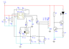
Yes, something is not right so i sent this message to the author
-------------------------------------
I have a concern regarding pin2 on the header pole connecting to pin6 (EN) on the IC
You said in another post about pin 2..."Yes, that is to Enable/Disable the chip (ON/OFF). So if I remember correctly you gonna connect it to the VCC (Input) to enable the chip. Datasheet sample circuit also confirms this."
But in your schematic Pin2 on the header pole (1,2,3,4) is listed as Output Ground and it is directly connected to (EN IC-pin6) with an in-line 180k resistor. Whereas in the datasheet example (EN IC-pin6) goes to ground but is paralleled with a 500k resistor to (IN IC-pin2) which goes to the voltage INPUT.
To explain further your header pole pinouts
1= output positive (from L2)
2= output ground (Goes directly to EN IC-pin6 with a 180k resistor in series)
3= input ground (directly to ground)
4= input positive (goes directly to IN IC-pin2
In summary I think the resistor in your schematic (R6 180k) should be paralleled between header pole pins 2 & 4
-------------------------------------
 
Authors response:
------------------------
Yes, the EN pin is separated for you to decide. so if you want to Enable/Disable the chip from outside, you will use it, otherwise, if you wanna enable the chip by applying the input voltage, you should just short pin 2 to pin 4. My mistake is on the backside silkscreen I think, where I have market 1 as input and 4 as output. sometimes because of tiredness happens. I'm a single person. however I test the whole structure and circuit always and then I publish. typo mistakes can happen. so you can compare with the schematic (PIN-1=OUT, PIN-2=EN, PIN-3=GND, PIN-4=INPUT), PIN-1 mark on the Silkscreen is correct.
------------------------
So this is interesting. Call me a slow learner but this is not a ground but a switch. I would like to implement a switch into this. Not so much in the circuit but externally. Ive added the switch to my schematic.
Buck07.png
 
I would like to implement a switch into this.
OK; also add a resistor from connector pin 2 to 0V, so the enable is pulled to ground when your external switch is off.

The input on the IC is obviously high impedance to work via 470K, so it's likely to be sensitive to noise and static if left unconnected when the switch is open. 10K or something around that should be OK and provide some "wetting" current for the switch; it could be up to 100K or more if current consumption is critical.
 
Status
Not open for further replies.

Latest threads

New Articles From Microcontroller Tips

Back
Top