Continue to Site

Welcome to our site!

Electro Tech is an online community (with over 170,000 members) who enjoy talking about and building electronic circuits, projects and gadgets. To participate you need to register. Registration is free. Click here to register now.

  • Welcome to our site! Electro Tech is an online community (with over 170,000 members) who enjoy talking about and building electronic circuits, projects and gadgets. To participate you need to register. Registration is free. Click here to register now.

How to reduce dissipation in hi side fet driver?

Status
Not open for further replies.

Flyback

Well-Known Member
Hi,
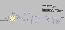
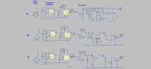
In the attached hi side fet gate drive circuit, do you know how I can prevent so much off-state current flow in D3 and R16?
I dont wish to reduce the value of R16 as i need high base current so i get high collector current.
(LTspice simulation and jpeg scm attached)
 

Attachments

  • Gate Drive cct _f.jpg
    Gate Drive cct _f.jpg
    138.3 KB · Views: 187
  • Full voltage drive transformer2_60khz_f1.asc
    5.5 KB · Views: 172
Dumb question. Why are you doing highside switching control using discrete components instead of a half bridge gate driver? I'm truly a hobbyist and would use one of the many driver ICs instead of this way.
 
D3 is on average about 10mW, I don´t see an issue there.
R16 is there to make Q1 turn on during negative cycles and the value seems low, try making it as high as possible, and sorry it is up to you to know when that resistance is as high as it can go and why.

On an unrelated note, you are trying to be a hardware designer / engineer for as far as I remember, possibly over 10 years, and yet I really don´t think your skills and knowledge have improved much at all. If you came for an interiew and I had to choose between you and a fresh absolvent of a 5 year university course where only half is related to electronics and the rest is IT or CS, I would most likely choose that other guy for the job offer.
 
...also Dr Ray Ridley in his article "gate driver design tips" says that bootstrap high side drivers should not be used in offline power supplys.....since they arent rugged enough.
That depends on which driver we are talking about, and what was the year when said Mr. Ridley made that note, could be decades old.
Recently I designed my personal project with ISO5851 IGBT driver. Yes it costs a lot ($1.5 each, but for production it is likely a no go), but I have no doubt that TI know what they are doing and that it will perform as per datasheet, and a bit beyond that. So for a small run or a one-off, it is much more economical than designing a gate drive transformer and associated circuitry from a scratch. For small volume it would still be better to copy a proven circuit from some name brand VFD or high end server power supply instead of designing one from scratch.
 
Thanks, this is for LLC, so its always 50% duty. I must admit, all of the offline power supplies of sucessful products, from 100's to 1000's of Watts , that ive taken apart to look into, are using Gate drive transformers.
 
Last edited:

Attachments

  • Best GDTs for LLC FETs.asc
    23.4 KB · Views: 168
  • Best GDTs for LLC FETs.jpg
    Best GDTs for LLC FETs.jpg
    167.4 KB · Views: 172
I often do not use the transformer for power but for the signal. Q1, Q5 amplifies the current. C1 is important. Must be there. Can you see why?
1651275565021.png

I like Coilcraft.com gate drive transformers. Toroidal with triple insulated wire.
 

Attachments

  • Gate Drive Transformer.asc
    6.9 KB · Views: 175
Some mechanism on the secondary to disable gate drive output until there is sufficient voltage stored to drive the transistor properly is also something that you better implement. At low duty cycles it will prevent the transistor to from turning on just partially.
 
BTW look up how tesla motor drive inverter works, no GDTs to be seen.
Thanks, yes, as you know, they are lower frequency and the switching transition not as fast though
 
Last edited:
I often do not use the transformer for power but for the signal. Q1, Q5 amplifies the current.
Thanks, very much agree, the method with the GDT just used to carry the signal and then uses a hi side supply is by far the best way to do it.....though its too many components.......from reverse engineering PSU's i know it can be done ( and done well) with just a single GDT, and no "hi side supply" method.

Thnaks, yes i appreciate the need for good supply decoupling, thanks.....also, please may i ask, did you use the npn/pnp totem pole instead of a hi side gate driver because the "logic low" voltage is one diode drop negatove of hi side ground...and you didnt want to damage a gate driver IC input by going below "Ground"?...i think the pnp/npn needs a series 10r to prevent shoot thru......and then when you use the 10r....you think a gate drive ic is better?
 
Last edited:
I have used high side drivers powered by a transformer. Sometime a full wave bridge to power the IC.
Many years ago....... I used "base drive" transformers before power MOSFETs were really available. Then I switched to MOSFETs.
When you have 2A gate current in the transformer you will have ringing. So by suing a two transistor current amplifier the transformer does not see the high turn on/off current. So the leakage inductor does not get charged up.

I thought you would come back and ask why Q1-C goes no where?
 
also, please may i ask, did you use the npn/pnp totem pole instead of a hi side gate driver because the "logic low" voltage is one diode drop negatove of hi side ground...and you didnt want to damage a gate driver IC input by going below "Ground"?
Have you ever seen a logical IC that does not tolerate inputs going at least 0.3v below the supply gnd? Or analog IC for that matter?
.i think the pnp/npn needs a series 10r to prevent shoot thru......and then when you use the 10r....you think a gate drive ic is better?
You mean series to the gate of your FET? Having a dead time between positive and negative pulse on the GDT would be my choice. I mean, referring to post no. 10, you need a circuit that when voltage at L10 is positive C1 charges and Q1 is allowed to turn on the gate. When the voltage at L10 drops below 0.7V Q5 is actively driven using energy from C1 to discharge the gate.
Then the opposite polarity pulse comes and things go the same for the other transistor in the half bridge, while the circuit described above still actively keeps the gate connected to source since the L10 voltage is still below 0.7V.
 
Thanks, yes, as you know, they are lower frequency and the switching transition not as fast though
Lower frequency than what? I have no idea what frequency they use, but somewhere in the 50k-100k Hz would be my guess at that power. And I have no idea what you are planning or comparing them to.
 
Thanks, but as you know, a BLDC motor drive for a car wouldnt likely be at 50-100Khz.
Eddy current losses in the stator and rotor would be too much .
Probably 20kHz max.
 
Tesla motor is not a straight BLDC, see this for example.
But anyway at say 20k RPM the driving voltage should be a 166hz sine wave since it is a two pole motor. Obviously you don´t push he output of each half bridge straight into the motor winding, you use a series inductor as if it were a synchronous buck converter. Then the high frequency losses are bound to your nice inductor material, and the motor only sees the 166hz sine waves.
 
Thansk, i am aware of current source BLDC's, where there is an inductor upstream, however, the majority voltage mode BLDCs do directly switch the motor coils...no additional inductor.
 
Status
Not open for further replies.

Latest threads

New Articles From Microcontroller Tips

Back
Top