Continue to Site

Welcome to our site!

Electro Tech is an online community (with over 170,000 members) who enjoy talking about and building electronic circuits, projects and gadgets. To participate you need to register. Registration is free. Click here to register now.

  • Welcome to our site! Electro Tech is an online community (with over 170,000 members) who enjoy talking about and building electronic circuits, projects and gadgets. To participate you need to register. Registration is free. Click here to register now.

How is this IC being used please? Beginner's question.

Status
Not open for further replies.
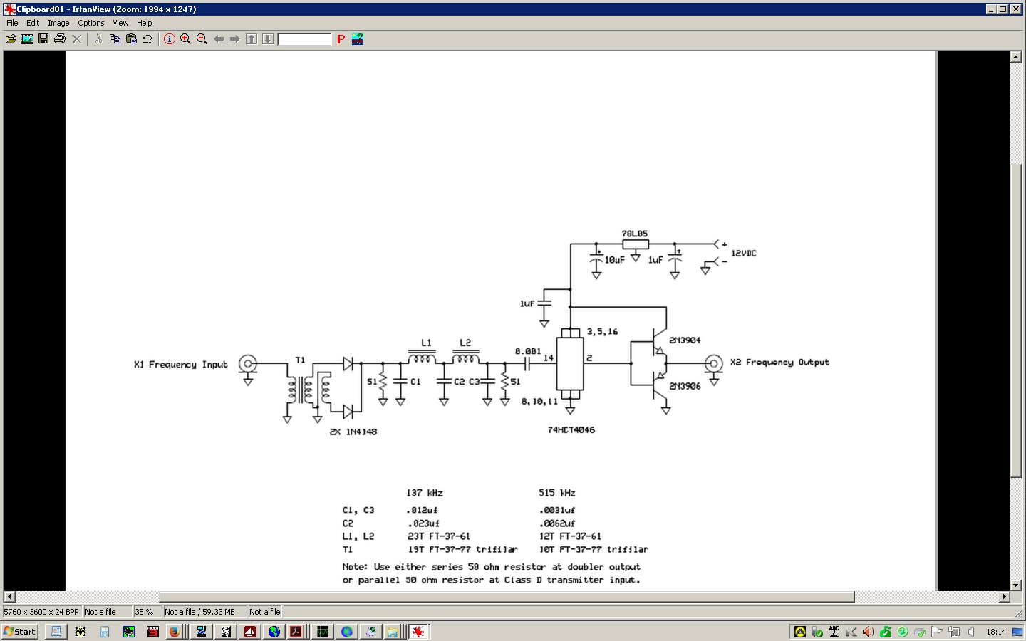
Attached is the schematic of a frequency doubler. It takes a 136kHz input and doubles it to give a 472kHz output. I am not sure how the IC and the two transistors function. The IC is a 74HCT4046 and its data sheet is available here: https://www.farnell.com/datasheets/66679.pdf?_ga=1.131595913.701848857.1475733716

Finally, as a beginner I am unsure about the note on the schematic regarding a 51 Ohm resistor, I assume it's for impedance matching, but what I don't understand is why it would be a series resistor at the doubler's output, but a parallel one on the Class D amp input. Thanks
doubler.jpg
 
The frequency doubling is done at T1 and 2x1n4148.

The IC has two options.
1) Maybe only a very small part of the IC is being used as a buffer. So it is just an amplifier. Used to sharpen up the edges of the signal.
2) There is more to the schematic. The other pins for the IC are on another page. It is a Phase Lock Loop. So this is a good place to put one.
 
It takes a 136kHz input and doubles it to give a 472kHz output.
2 x 136 = 272 not 472

As Ron has said the doubling is done in T2 and the 1N4148s.

L1, L2, C1, C2 and C3 form a lowpass filter with a cutoff frequency around 270kHz.

The connection of the '4046 is strange, my best guess is that one of its phase detectors is being used to create a square wave from the 272kHz (?) coming from the filter.
Grounding pin 10 of the 4046 is also strange, this is an output. The datasheet specifically states that if the output is unused, it should be left disconnected.

The two transistors are being used to give mode drive current to whatever it is connected to.

As for the note about the 51 Ohm resistor, I don't know why the two different connection options are given.

Where did you find this circuit, there are some strange inconsistencies.

JimB
 
Attached is the schematic of a frequency doubler. It takes a 136kHz input and doubles it to give a 472kHz output. I am not sure how the IC and the two transistors function. The IC is a 74HCT4046 and its data sheet is available here: https://www.farnell.com/datasheets/66679.pdf?_ga=1.131595913.701848857.1475733716

Finally, as a beginner I am unsure about the note on the schematic regarding a 51 Ohm resistor, I assume it's for impedance matching, but what I don't understand is why it would be a series resistor at the doubler's output, but a parallel one on the Class D amp input. ThanksView attachment 104292
Hi CW,

As Jim says in post #3, the two transistors form a classic output buffer: the NPN transistor provides the source current to drive a low impedance interface (sounds like 50 ohms in this case) and the PNP transistor provides the sink current. To a first approximation, the output impedance of the buffer is zero ohms.

You would put a 50 ohm resistor in series with the buffer output to make the output impedance of the buffer 50 ohms to match the 50 ohm impedance of a coaxial cable, for example. This is called back termination and, if the receiving end is also 50 ohms, would result in halving the signal voltage amplitude (this is normal with back termination).

Matching impedances prevents reflections which would distort the waveform.

It is odd that the instructions do not mention making the input to the class D amplifier 50 ohms also.

The second option, to just terminate the class D amplifier input with 50 ohms and leave the buffer output unterminated, would not halve the waveform voltage amplitude.

In this case a zero output impedance buffer would be feeding a 50 ohm line (say coax cable). This will work fine because a zero impedance source will absorb all of the reflections just the same as a 50 ohm source.

spec
 
Last edited:
Looks like they are using the 4046 Pll just as a driver for the o/p devices.
If so it might be a case of what happened to be in the junk box at the time.
 
Attached is the schematic of a frequency doubler. It takes a 136kHz input and doubles it to give a 472kHz output. I am not sure how the IC and the two transistors function. The IC is a 74HCT4046 and its data sheet is available here: https://www.farnell.com/datasheets/66679.pdf?_ga=1.131595913.701848857.1475733716

It appears that most of this IC Is not being used. If you look at the Fig 5 in the datasheet. you'll notice that your signal is going into Pin 14, and coming out Pin 2. The only active 'control' signal is the signal coming in from pin 3. This is tied high on your schematic. Since this feeds, without inversion, into the XOR Gate, the XOR function will always see a '1' on the lower input. As a result, SigIN will always be inverted going out of PC1Out.

I don't know if you're trying to figure out a replacement or not, but I see also no reason why you also couldn't just drop a more common 74HCT gate in there. (adjusting the wiring accordingly) I'd probably use either a 74HCT04 or 74HCT14. You may also be able to get away with a 74HC series instead of a 74HCT series. I'd have to understand a bit better the signal conditions at the input to the gate. If it was on my workbench, I'd build the first part of the circuit, stick a scope on it and make a judgement call.

Since this is a beginner question, I'll add a bit more information for you about the differences in the gates I suggested above. if you already know this, just ignore:

To operate correctly, The 74HCT series needs low voltages to be below 0.8V and high voltages to be above 2.0V. 74HC needs the lows below 1.3V and the highs above 3.7V (at 5V operating voltage, 3.3V is different). It's important to make sure your input thresholds match the signal you're putting into them. Which is why I said above that you could drop a 74HCT series gate in there (since the existing chip is a 74HCT chip), and that you *might* be able to put a 74HC in there - it all depends on the amplitude of the signal out of the doubler.

The Difference between a 74HC*04 and a 74HC*14 is that the 04 requires the signals to transition from low to high quickly or else you will often get stray pulses. A 74HC14 has what is called 'Schmitt trigger' inputs which due to the way they are constructed, will generally help clean up slowly transitioning signals. Because I generally am using an inverter for the purpose of bringing in outside signals to a circuit, I for the most part use the '14 variant pretty much everywhere. I would have to look at the datasheets in more detail to see if for very high frequency circuits there is any meaningful difference in performance between the two - it would not surprise me to find that one or the other does better above a certain frequency.

I can also answer the '50 ohm' resistor question....

The circuit apparently expects you to use a 50 ohm transmission line (i.e. coax, but it's also the connectors on both ends, the pcb etc.). When you put high speed signals down a transmission line you have to be careful to correctly terminate the transmission line. If you don't terminate the transmission line, once the signal reaches the far end, a portion of it will bounce off the far end and return back to the transmitter. I don't want to go into all of the details of how this is bad - but it is. Let's just say that you really want to prevent this.

There are two ways to do this:

1) Provide a *parallel* termination at the far end (aka receiver)
2) Provide a series termination at the near end (aka transmitter)

One could debate the merits of both options. In this case, I'd probably choose to add the 51 ohms at the receiver (class D amp?) just because I could then use a signal generator from the bench and have it be terminated correctly.
 
What a great forum, and what a great selection of detailed replies, thank you all very much indeed. I have spent a lot of time pretending I am knowing what I am doing to stop FET failure in the low frequency power amp that this pre-amplifier and doubler feed, and in a previous, quite different design, and I believe I have now found the issue. The same designer of the doubler suggested i use part of the schematic from another of his designs to build a pre amp. I have a Kenwood TS-590 transceiver for ham radio usage and I operate a lot on the 136kHz LF band. This transceiver only has the facility to give a circa 0 dBm output on this frequency. Due to the digital software i run, and the requirement of the push pull Class D amplifier to have 136 kHz times two as its input (272 kHz, sorry about the original typo...), I needed to double up the output frequency. The designer of the doubler stated that it needed between +7 and +20 dB input, here:

http://www.w1vd.com/X2LinearClassDinterface.html

so I needed a pre-amp to go from about 0 dBm to at least +7 dBm.

He suggested using the tail end of another of his circuits and I assumed he meant the bit I have outlined in red:

preamp.jpg


I built this and the doubler, but found mysterious FET failures at the end of a TX session. The amp schematic is at:

http://www.gatesgarth.com/kw-amp.pdf


After much messing about i finally found out two days ago that the signal from the doubler to the input of the amp was NOT stopping cleanly at the end of a TX session, but was held high then stopping noisily. Again, after hours of messing i found reducing the drive from the transceiver into the pre amp, which I modded to reduce gain by changing the 1k feedback resistors to 2.7k ones, the glitch stopped. I have no more FET failures despite several hours of off and on transmitting and making my first ever UK to US trans Atlantic contact on 136 kHz. Gluing advice on here together has helped enormously, and I have linked to the various schematics on here in the hope anyone interested might critique things further. I am especially interested in the comments about changing to a Schmitt trigger IC made by ForrestC, and loathe as I am to ask for more, a little more detail on what a swap would entail would be great. I am guessing what was happening was the low signal to the 74HCT4046 device in the doubler wasn't going low enough and "funny things" were happening?Whilst all is well now, I have to wonder if I could, or should, optimise things better, especially the pre-amp and doubler. Do my 2.7k feedback resistors look like they should put gain in the right ballpark?


Sincere thanks to all for helping me finally resolve this long standing (and costly...) problem!!
 
Last edited:
Status
Not open for further replies.

Latest threads

New Articles From Microcontroller Tips

Back
Top