Athosworld
Member
I want to know how does a NES On A Chip (NOAC) work, if possible, who invented it and why.
How does that chip read the data from the cartridge and executes it like the real NES.
Is it just some kind of extremely integrated 6502 or an FPGA?
My theory: When the chip gets power, it inmediatly starts reading the contents from the cartridge/NOR flash on boot and through a series of logic gates, it generates an AV output to the TV.
Im planning to do a decap of the blob chip.
Most of these NOAC systems have a COB in the controller that I suspect is just a shift register that sends signal to the NOAC because it isn’t powerful enough to execute a game and read directly from the controller.
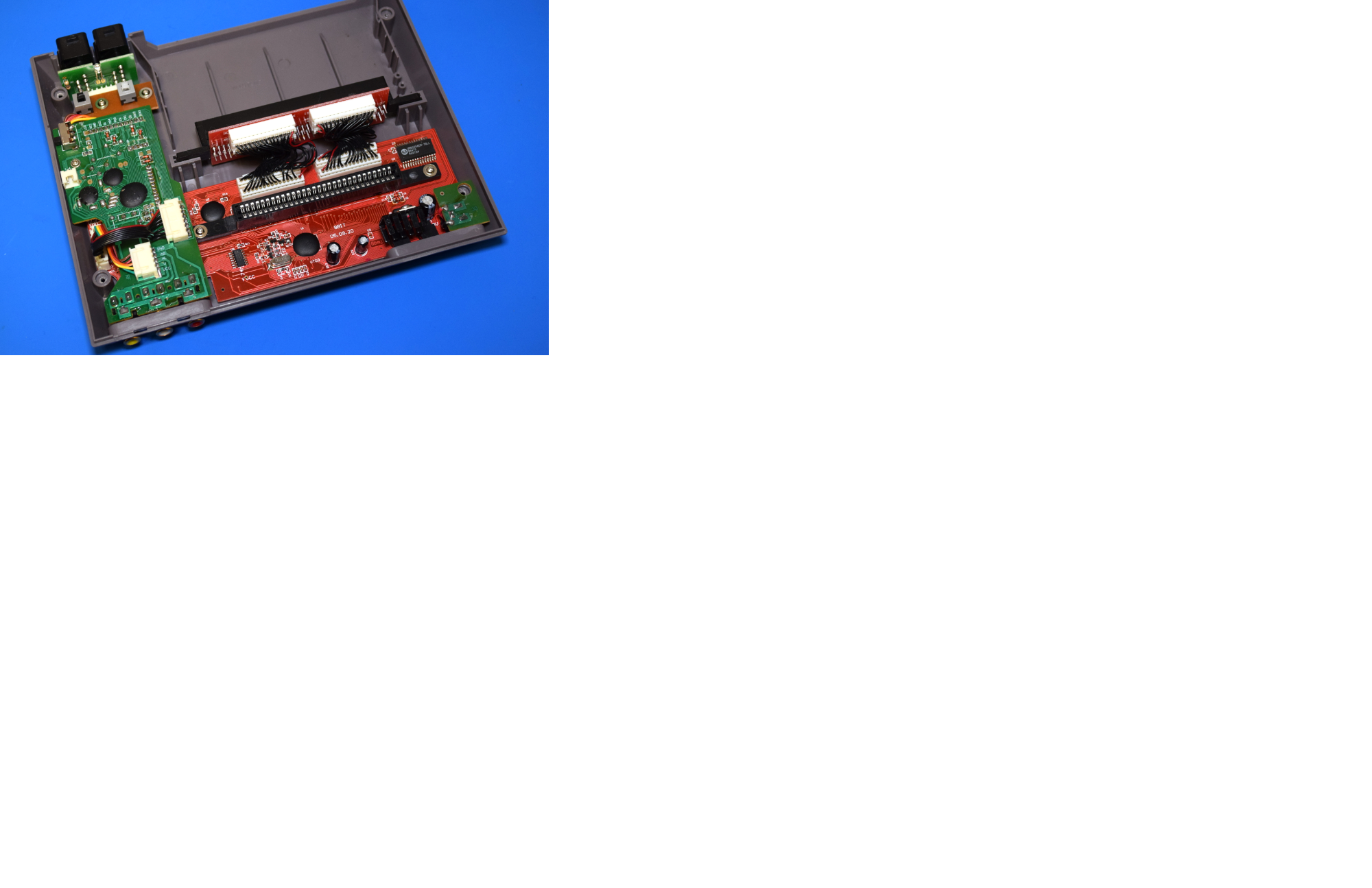
You can see in this photo by hackaday.io, a system with a variety of blobs, are the functions of a NOAC spread over these chips?


