Continue to Site

Welcome to our site!

Electro Tech is an online community (with over 170,000 members) who enjoy talking about and building electronic circuits, projects and gadgets. To participate you need to register. Registration is free. Click here to register now.

  • Welcome to our site! Electro Tech is an online community (with over 170,000 members) who enjoy talking about and building electronic circuits, projects and gadgets. To participate you need to register. Registration is free. Click here to register now.

High side switching vs low side switching

Status
Not open for further replies.

akahrim

Member
Hello All,

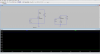
I am simulating a switch circuit using mosfets. I simulated two circuits. One with the mosfet on the low side and one with it on the high side. The mosfet is an NMOS FDC637AN. I chose this at random just because it was in the library. When the mosfet is placed on the low side the current is significantly higher than when placing it on the high side. When I do the math, it appears that the mosfet is in the triode region Vds<Vgs-Vth. Probing around the circuit Vds is .037V when placed in the low side configuration and 1.48 when placed in the high side configuration. I am stuck understanding why this is happening. Can someone please explain why the mosfet is able to pass more current when placed in the low side configuration? I have attached an image of the circuit that I simulated.
 

Attachments

  • High Side Switching vs Low Side Switching.png
    High Side Switching vs Low Side Switching.png
    69.7 KB · Views: 583
In the secvond circuit, the voltage at the source terminal of M2 is raised by the current through R2. This reduces the gate-source voltage to the mosfet so it doesn't turn on very well.

Change the connection of your V4 voltage source so that it's negative point is connected directly to source of M2, and you will see the two circuits behave about the same.
 
you are not turning on the high-side switch enough.
For high-side switching essentially the GATE must be brought Vth above the main voltage (in this case3.6+3.4 w.r.t. 0V) EITHER by having a larger voltage source OR via having a high-side driver, bootstrapped stage or a floating psu for the high-side switch
 
Hello ChrisP58,

Thank you for pointing out that design. I connected the negative terminal of V4 to the source and the circuit performed exactly them same in simulation. Thank you for pointing this out.

Hello Styx,

I've seen mosfet drivers and floating power supplies before but I'm not sure what a bootstrapped stage is. Would you able to point me in the right direction?

Thanks guys for your help.
 
ur terminology is wild, reckless, and brainless

theres no such thing as "high side" and "low side"

what you have there is a common-source circuit, and the second one is common source with source degeneration.
 
ur terminology is wild, reckless, and brainless

theres no such thing as "high side" and "low side"

what you have there is a common-source circuit, and the second one is common source with source degeneration.

au contraire mon frere

H-Bridges do have high sides and low sides. Either side (high or low) of an H-Bridge could be common-source (common-emitter) or common-drain (common-collector).
 
au contraire mon frere

H-Bridges do have high sides and low sides. Either side (high or low) of an H-Bridge could be common-source (common-emitter) or common-drain (common-collector).
Hi MikeMI,

Thank you for taking the time to send the application note. The link works perfectly.
 
In a nutshell, A bootstrap is a capacitor and diode that allows the gate voltage to stay the required voltage above the source voltage. You really need to learn this (read a lot) if your serious about electronics.

Back to the bootstrap -
1. A diode in forward bias from the gate supply voltage.
2. A capacitor of the correct value and voltage. The value is high enough to supply gate voltage for the "on" time of the high side mosfet.
3. One side of said capacitor is connected to pin VB of driver, the other to the source pin.
4.When the low side fet is on, the BS(boot strap) capacitor is charged to gate voltage through the diode.
5. When the low side is turned off, and the high side starts to conduct, the BS cap discharges into the VB pin of the driver, allowing the gate voltage to always be the correct level above the source voltage (Vgs). The diode stops the gate voltage from the BS cap from going anywhere but the VB pin of the driver.
 
thats a lot to read
can u give us a short common sense explanation of what bootstrapped means?

Sometimes the struggle is what you need to enhance your knowledge retention. Otherwise, the short version is good for you to pass a tests and "flush" all remnants of that knowledge out.
 
you are not turning on the high-side switch enough.
For high-side switching essentially the GATE must be brought Vth above the main voltage (in this case3.6+3.4 w.r.t. 0V) EITHER by having a larger voltage source OR via having a high-side driver, bootstrapped stage or a floating psu for the high-side switch
Using Vth as the Vgs voltage to turn on a MOSFET is a common mistake. Vth is the point at which the MOSFET is just starting to turn on. To fully turn it on Vgs needs to be much higher, typically 10V for a standard MOSFET or 3V-5V for a logic-level type MOSFET.
 
never said just to use Vth ;) I always drive my FET's with +/-15V unless their gate cannot tolerate it.
What I said was the gate had to be taken Vth above the main voltage w.r.t. 0V I didn't say to
 
In the secvond circuit, the voltage at the source terminal of M2 is raised by the current through R2. This reduces the gate-source voltage to the mosfet so it doesn't turn on very well.

Change the connection of your V4 voltage source so that it's negative point is connected directly to source of M2, and you will see the two circuits behave about the same.

Hi,

I have to agree that the high side has to be driven with a higher voltage than the power supply in order to get the MOSFET to turn on properly. This is a problem in all N channel inverters. Often we see P channel devices coming into play here intead.

BTW is that the M.C. Escher "Waterfall" as your avatar? I have one of his books, he did some very interesting art work. I also like "Relativity" and all of his other "3d" deceptive drawings.

Yes, it is Escher. I've always enjoyed his pseudo 3D stuff.
I keep trying, but haven't been able to build any of his models in Solidworks. lol
 
ur terminology is wild, reckless, and brainless

theres no such thing as "high side" and "low side"

what you have there is a common-source circuit, and the second one is common source with source degeneration.

Not true. A high side switch will be a P channel with the source being the source of a positive constant voltage.
A low side switch will be an N channel with the source connected to ground, thus switching it off will isolate the ground.

The high side switch can be used to power the entire circuit on and off. A low side switch can do similar but can cause problems with floating grounds when switched off.
A low side switch is great for switching bulbs on and off due to the fact most N channel FETs have a lower Rds on, but if you want to switch an ampliying stage for example can lead to a world of hurt.
 
Status
Not open for further replies.

Latest threads

New Articles From Microcontroller Tips

Back
Top