Continue to Site

Welcome to our site!

Electro Tech is an online community (with over 170,000 members) who enjoy talking about and building electronic circuits, projects and gadgets. To participate you need to register. Registration is free. Click here to register now.

  • Welcome to our site! Electro Tech is an online community (with over 170,000 members) who enjoy talking about and building electronic circuits, projects and gadgets. To participate you need to register. Registration is free. Click here to register now.

Help on reviewing design for clean ground

Status
Not open for further replies.

pavjayt

Member
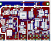
I am done redesigning my board which has both digital and analog sections. I tried to make sure they both have separate grounds and using ferrite beads between power supply grounds and circuit grounds. Any suggestions/improvements are greatly appreciated. Top & Bottom are ground planes while middle layers are power. (+5 within digital section - far right & +/-15V in the middle & +/-5V to the left). I know its not as simple to figure out ground noise, but wondering if you see anything that's obvious that needs to be improved.

Let me know if you need actual board file (done in eagle).

thanks
 

Attachments

  • temp.pdf
    414.9 KB · Views: 247
That layout looks nice, what PCB program did you use?
 
For absolute lowest noise the digital and analog ground planes should not overlap since layer to layer capacitance can couple noise between the two.
Better to use a split plane on the same layer with a single point connection (with a ferrite bead if desired) between the two.
 
Hmm, Yup I missed that. Eagle does a good job on layouts. Hey Pav, how many layers is your board?
 
Hmm, Yup I missed that. Eagle does a good job on layouts. Hey Pav, how many layers is your board?
Not sure how good it does, but the whole layout is done by me, no help from eagle automated routing as I didn't like its initial results in the beginning.
 
For absolute lowest noise the digital and analog ground planes should not overlap since layer to layer capacitance can couple noise between the two.
Better to use a split plane on the same layer with a single point connection (with a ferrite bead if desired) between the two.

In the picture you can see the split ground planes and they are connected with a ferrite bead under AD7533 (not seen in the picture) and with in the power supply section, I have ferrite beads connecting main ground to digital ground and also for 5V from LDO to 5V power plane. Same with all power planes in other sections.

Other thing that I am debating on is whether to use an inductor in place of ferrite bead. Also adding more 0.1u caps in all source power sections.
 

Attachments

  • Digital_analog_grounds.png
    Digital_analog_grounds.png
    350.8 KB · Views: 193
Last edited:
Other thing that I am debating on is whether to use an inductor in place of ferrite bead. Also adding more 0.1u caps in all source power sections.

I would stay with ferrite bead if I were you. You want this component to be very lossy at high frequencies. Ferrite beads fit that job perfectly, inductors not.
 
I would stay with ferrite bead if I were you. You want this component to be very lossy at high frequencies. Ferrite beads fit that job perfectly, inductors not.
Thanks, will stay with Ferrite beads, another thing that I am thinking about is whether a 1206 package ferrite beads that I am currently using suffice the current requirements for the power planes?

How about ground vias that I placed all over the board connecting top gnd to bottom gnd planes? Am I overdoing them?
 
Whats the PN for the bead? The datasheet should give you that info.
 
One thing, when selecting the fer-rite bead, you should consider the unwanted frequencies you want to keep out of you circuit. The bead your using is a high frequency bead, and if your EMI is below 20 MHz or so, you may want to consider another bead. Just a thought:)
 
Thanks for the tip, will look into it. My max frequency of the signals in digital section is 16KHz and in my analog section is 20MHz.
 
One thing, when selecting the fer-rite bead, you should consider the unwanted frequencies you want to keep out of you circuit. The bead your using is a high frequency bead, and if your EMI is below 20 MHz or so, you may want to consider another bead. Just a thought:)
I found one that is rated at 32Ω at 1MHz PN#**broken link removed**, but when I check its datasheet it says inductor type. Not sure which one to select from here, trying to find one at 1A rating with the lowest frequency which happens to be 1MHz. Any suggestions for a part?
 
The Kemet catalog sucks, most manufacturers provide impedance graphs for their beads, so you can see how the function over frequency. I would look at a Murata catalog. The Kemet part might work but it hard to say without knowing how it functions on the low frequency end. I have discovered that F-bead performance is not linear as you might expect from the formula for XL.
Anyways this Bead is 2 A. 1000 ohm at 100MHz. Z1206C501BPWZT KEMET part.
 
This chart may help. From the Murata website.
bl_img0002.ashx
 
Thanks Mike, after hours of looking around for those parts on Digikey where most of them are not in stock, I am having a hard time to choose. I am trying to find BLM-AX series rated at around 500mA, but couldn't find them in stock. The ones that I narrowed down based on the current rating and frequency are here. Not sure which one to choose.
 
I would stick with the 1206 package that you have already laid out your board for. I would not overthink the bead, although putting in some work is important. I messed around with the selection criteria in Digi-Key. This gives more options in 1206 BLM family by Murata. Pick one from the list, you could always change it after the build based on testing.
https://www.digikey.com/product-sea...t=0&page=1&quantity=0&ptm=0&fid=0&pageSize=25
 
Status
Not open for further replies.

Latest threads

Back
Top