Electro Tech is an online community (with over 170,000 members) who enjoy talking about and building electronic circuits, projects and gadgets. To participate you need to register. Registration is free. Click here to register now.
Welcome to our site! Electro Tech is an online community (with over 170,000 members) who enjoy talking about and building electronic circuits, projects and gadgets. To participate you need to register. Registration is free. Click here to register now.
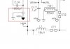
Could anybody explain the Schematic connection marked in Red. This ckt is of a Microcontroller board with different pins having different ground planes. But I cannot understand this connection shown. It cannot be a short ckt or else you would not need a different symbol in the first place (I suppose).
I would suggest the black triangles are a separate ground point, like you often have with separate analogue and digital grounds. The normal ground shown may be where the PLL ground is connected to the normal ground?.
This is the method used to route pcbs when digital (noisy) and analog (hopefully not noisy) ground planes need to be kept separated.
In order for the circuit to work electrically, the grounds must be at the same potential, but to prevent the noisy digital currents from flowing along the analog ground plane, the intertie can only happen in just one place
This is the single point grounding principle. If you do not understand this principle, you have no business designing mixed signal analog-digital systems.
This site uses cookies to help personalise content, tailor your experience and to keep you logged in if you register.
By continuing to use this site, you are consenting to our use of cookies.