riccardo
Member
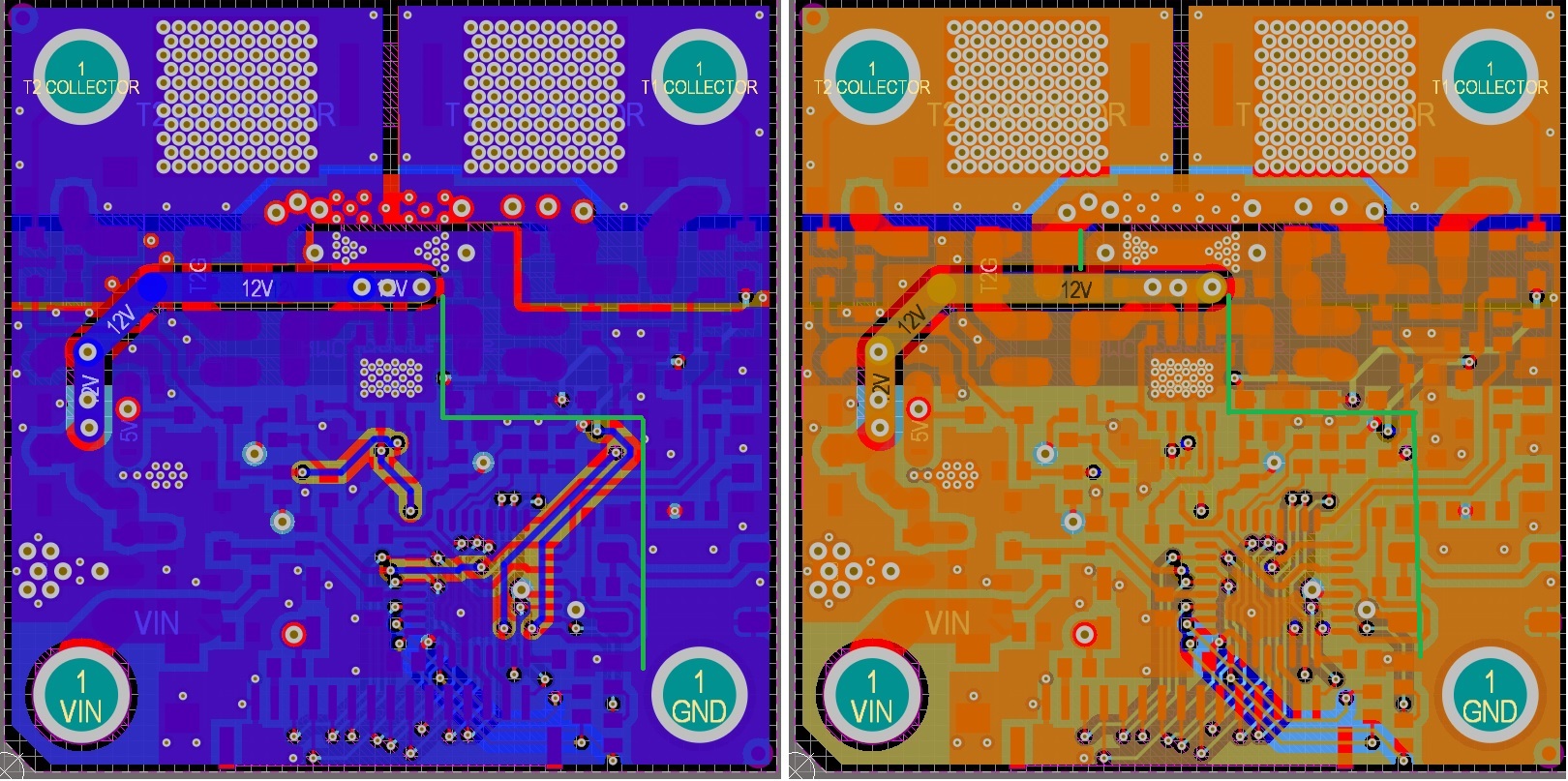
Hello, I am working on a high density circuit where space is very limited. It is 4 layers, with bottom GND, and a mid GND. The power electronics will carry 20 Amps. The image below shows the ground polygons I have. I am wondering if I should split the polygons as indicated by the green line.
There's enough copper there to carry the current (2oz traces). Will this help reduce interference from the large ground current mixing with the signal currents? The part in the centre with the vias is the MOSFET driver. The two patches at the top are power MOSFETs. The vias in the triangle shapes are the MOSFETs connection to GND

There's enough copper there to carry the current (2oz traces). Will this help reduce interference from the large ground current mixing with the signal currents? The part in the centre with the vias is the MOSFET driver. The two patches at the top are power MOSFETs. The vias in the triangle shapes are the MOSFETs connection to GND
Last edited:

