Electro Tech is an online community (with over 170,000 members) who enjoy talking about and building electronic circuits, projects and gadgets. To participate you need to register. Registration is free. Click here to register now.
Welcome to our site! Electro Tech is an online community (with over 170,000 members) who enjoy talking about and building electronic circuits, projects and gadgets. To participate you need to register. Registration is free. Click here to register now.
Thanks Eric.
I can manage to add attachment per your direction.Thank you very much.
I just issued a new post whose title is:Making a output voltage,Would you like to review it when are feel free.Thanks in advance.
take a look at the datasheet for the mosfets used. they should have a body diode in their and you need to make sure that the reverse em will not damage the body diode. if not, put some diodes on those mosfets.
Getting back to the blown FETs.
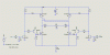
What are the part number of both the P and N channel FETs on the diagram? The datasheet, and knowing the voltage of Vbat, might give us more of a clue.
I know it has been mentioned that the failure points towards a gate-source breakdown, but this circuit could self destruct when it is used. ie: If both PWM inputs are low, nothing happens. If only one PWM input is "high" the motor will run and nothing bad should happen. If both PWM inputs are "high" then all four FETs are turned on and smoke happens!
In the circuit shown, no bulk bypass is shown on Vbatt. If this isn't close enough to the H-bridge or has been altogether forgotten, then Vbatt will be spiking seriously. The P-channel devices will get the worst of it, and will die very quickly.
If Vbatt is 12V or so (gotta guess), and guessing that the motor is less than 6A (R45 is .02 ohms 0.5W) I would use 220µF in parallel with a couple of 1µF ceramics.
[edit] I should mention if Vbatt is an automotive supply, then 14.4V is too close to the breakdown rating of a lot of mosfets and the design needs surgery. I cannot find a listing for a GB3318 or GA3055 mosfet, am I reading them correctly or are these house numbers?[/edit]
Thank you for your reply.I admit that I can't express my problem in detail,so let you have trobule in understanding.
I decide to update my problem later,hope you can give me more analysis and comment.Once again,I learn a lot from you.Thank you very much.
Thank you for your reply.I admit that I can't express my problem in detail,so let you have trobule in understanding.
I decide to update my problem later,hope you can give me more analysis and comment.Once again,I learn a lot from you.Thank you very much.
Hi Eric
1. VBAT is 9.6V.
2. GB3318 datasheet is belowing:
BVDss is -25V, Rds(on) is 150mohm,Id is -10A.
3. GJ3055s datasheet is belowing:
BVDss is 20V, Rds(on) is 25mohm,Id is 18A.
detail please refer to the attachment,there is only GJ3055s specification.I will add GB3318 specification here when I get it.
One more thing need you know,the bad mosfet is only GB3318,not GJ3055s.
update my problem: Gate and source of mosfet is short
My problem is that the PCBA whose the bad PMOS
(GB3318) can be pick out by the testing jig.Now I need to analyse why the mosfet GB3318 is damage.
The testing jig setting is belowing:
1.DC Power supply is 10V~15V,often use 12V.there is stable voltage output 6V to PCBA VBAT.That means 6v to the PCBA.
2.Use 11ohm 10W resistor replace of the motor,so there is no motor in the testing jig.My understanding is no reverse EM on the PCBA.
3. IC PWM comes from Logic IC,there only one channel IC PWM will output high level.Two channel IC PWM have never output high level at the same time.
4.Severals E.Cap(220uf and 470uf) connect VBAT to ground.
That's all.would you like to hele me ananlyse why GB3318 mosfet is damage.its Gate and Source is short.
can you post some captured waveforms while in test? Show the gate, drain and source of the PFET simultaneously (can be referenced to ground) while switching on and when turning off. If you have 4 channels, show the gate of the lower FET as well.
I saw it Eric, but he forgot that the inductors he used in series are enough to create the back emf. perhaps the motor is substituted by the combination of these inductors and the 11 ohm.
However 5.6uH is too small to be expected as Motor simulator.
I saw it Eric, but he forgot that the inductors he used in series are enough to create the back emf. perhaps the motor is substituted by the combination of these inductors and the 11 ohm.
However 5.6uH is too small to be expected as Motor simulator.
This site uses cookies to help personalise content, tailor your experience and to keep you logged in if you register.
By continuing to use this site, you are consenting to our use of cookies.