Electro Tech is an online community (with over 170,000 members) who enjoy talking about and building electronic circuits, projects and gadgets. To participate you need to register. Registration is free. Click here to register now.
Welcome to our site! Electro Tech is an online community (with over 170,000 members) who enjoy talking about and building electronic circuits, projects and gadgets. To participate you need to register. Registration is free. Click here to register now.
Because the intrinsic base resistance is multiplied by the current gain (Hfe) in the CE configuration to give a higher effective input impedance but it's not (amplified) in the CB configuration.
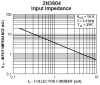
The datasheet for the 2N3904 has a graph of its typical common-emotter input impedance when its emitter is grounded or is bypassed to ground with a capacitor. Of course the biasing resistors are parallel to the input impedance.
The input impedance changes when the collector current changes:
This gives a good mathematical /graphical idea
But what exactly is happening with the electrons and the holes?
Does the biasing of the transistor play any role?
And I have another doubt
Once the Q point is fixed and v apply an ac signal does it have a dc component too or is the average of the signal equal to zero since it varies from the q point?
This site uses cookies to help personalise content, tailor your experience and to keep you logged in if you register.
By continuing to use this site, you are consenting to our use of cookies.

")