Continue to Site

Welcome to our site!

Electro Tech is an online community (with over 170,000 members) who enjoy talking about and building electronic circuits, projects and gadgets. To participate you need to register. Registration is free. Click here to register now.

  • Welcome to our site! Electro Tech is an online community (with over 170,000 members) who enjoy talking about and building electronic circuits, projects and gadgets. To participate you need to register. Registration is free. Click here to register now.

Eagle - strange way treating layers

Status
Not open for further replies.

Boncuk

New Member
Hi all,

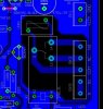
I finished a single layer board today marking an area around a mains switching relay using layers 40 (bKeepout) and 42 (bRestrict).

Then I drew a rectangle (polygon) using layer 16 (Bottom) around the entire board and called it "ground". What a great result! :mad:

Eagle just ignored the bKeepout and bRestrict! There were ground fills all over the board including the mains power part (certainly a source of malfunctions and shorts).

This phenomenon happens with every Eagle version, even the latest.

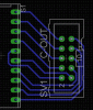
Here's how to get around the problem: Draw a polygon of least wire width (I used 0.1mm) around the area you don't want to be filled with ground using layer 15 (Bottom). Then call it anything - but not GROUND! (I called it: KEEPOUT :) )

Draw your next polygon (or rectangle) using a "normal" trace width. Call it ground and this is what you get. (Attachment)

Don't forget to adapt the DRC rules accordingly. You'll get a never ending error list when not setting the minimum trace width to the value you have used to KEEPOUT.

Regards to all

Boncuk

Edit: You can't name a polygon drawn with layers 40 and 42!
 

Attachments

  • keepout.jpg
    keepout.jpg
    30.5 KB · Views: 253
Last edited:
Works as it always has; I just went and checked on my system. Rectangles and polygons are not interchangeable.

Polygons are used for fills. They follow spacing rules on 1 & 16. They are ignored on layers 40 & 42.
Rectangles are used for restrict. They work on 40 & 42, but are imo not very useful on 1 & 16.

Yes it's a pain building the type of restrict area shown in your example out of rectangles.
 
Last edited:
I've never even noticed this, since I've always used rectangles for restrict areas. It would be nice to be able to make a polygon restrict area. Thanks for the solution Boncuk.
 
Last edited:
Sorry to piggyback on your post, but I'm new here and not allowed to start a new thread.

I'm working on a pcb design in Eagle 5.6 and I'm having a problem.

My trace widths and pad sizes will not permit lines to be routed between the pads of a DIL14 package. I can route every signal on my board except one with my current settings. I would like to make two pads on the DIL14 just a bit smaller than I can route a thinner line through and I'm good.

It's easy enough to route a new signal and choose the width, but I cannot seem to find a way to make two pads on the DIL14 a bit smaller without creating a new package in a library. If anyone knows of a way to accomplish this without creating a new part that would be great.

Assuming I have to create a new package, I cannot seem to copy an existing DIL14 and copy it so I may modify the two pads. Every time I group/copy (or cut) and then try to paste I get "Buffer Empty". Very frustrating...

I suppose I can create a new DIL14 package from scratch, and this may be what I need to do, but I thought I would ask if anyone has a more simple approach to my problem first.

Thanks.
 
Last edited:
You can edit the current package you are using. Just open it and resize the pads you want, or,

..you can copy the part to a new library, or just copy it to another package within the same library. Copying and pasting is pretty unintuitive in Eagle. The easiest way to copy something from one library to another, is to open the library you want to copy to. Then go to the main control panel. Open up the library tree, right click the package you want to copy and select 'copy to library'. It'll paste the item into the currently open library.
 
Hi tswan,

DIL-packages have a pin spacing of 0.1 inch (2.54mm). If you start designing a PCB Eagle standard grid size will be 0.05 inches (1.27mm). That should be exactly the space required to route a trace between IC-pins.

A grid size of 0.05 inches might become too large if many traces have to run parallel with limited space. (trace distance 0.05 inches)

So you might use the next smaller grid size of 0.025 (0.635mm) or even 0.0125 (0.3175mm). The latter will be unusable for trace width >0.00394 inches (0.1mm)

Changing grid sizes you should keep in mind to always use numbers with an exact integer division factor. E.g. changing from grid size 0.05 to 0.024 inches will result in a faulty design (not speaking of OFF-GRID and ANGLE errors when performing a design rule check (DRC))

Copying packages is very easy. Just follow these steps:

Group the package including the information contained in layer 21 (tPlace, normally '>NAME' and '>VALUE'). Then cut the group to the paste buffer.
Close the library and open the one you want to copy the package to.

Select "package" --> "new" and type in the name, e.g. DIL-08. Answer the following question: "Do you want to create a new package?" by clicking "Yes".
A new window opens and you just drop the package (out of the paste buffer) onto the screen. Make sure it is centered around the 0/0 coordinate cross. It is easier to move on the PCB design and Eagle3D wants the packages centered around the 0/0 position as well. Save the library.

That's it.

One remark: Study the Eagle manual to get on well. Eagle is really what the abbreviation stands for: Easily Applicable Graphic Layout Editor.

Boncuk
 

Attachments

  • GRIDSIZE.gif
    GRIDSIZE.gif
    23.9 KB · Views: 197
Last edited:
Hi Boncuk.

@tswan. With the default grid settings as pointed out by Boncuk, .16mm and lesser width wires are easy to route between DIL/DIP package pins.
 
Hi Boncuk.

@tswan. With the default grid settings as pointed out by Boncuk, .16mm and lesser width wires are easy to route between DIL/DIP package pins.

Hi Wond3rboy,

in fact you can use a trace width of 0.4064mm. There is still more than the standard minimum distance of 0.2032 initially set by the DRC.

The clearance (distance between pads and traces) is determined by
pin distance (2.54mm) minus 1X pin diameter (standard for DIL-packages 1.6002mm minus trace width (0.4064) divided by two, which results in 0.2667mm distance between trace and pad.

Using a trace width of 0.15mm you might route two traces between two IC-pins using a grid size of 0.15875mm (0.00625inches) still getting more than the minimum distance of 0.2032mm (0.21326~)

It's done with industrial PCBs.

Boncuk
 
Status
Not open for further replies.

Latest threads

New Articles From Microcontroller Tips

Back
Top