Continue to Site

Welcome to our site!

Electro Tech is an online community (with over 170,000 members) who enjoy talking about and building electronic circuits, projects and gadgets. To participate you need to register. Registration is free. Click here to register now.

  • Welcome to our site! Electro Tech is an online community (with over 170,000 members) who enjoy talking about and building electronic circuits, projects and gadgets. To participate you need to register. Registration is free. Click here to register now.

eagle routage pcb component placement

Status
Not open for further replies.

maryem

Member
hello,
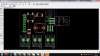
i 'm doing a 39x39mmcircuit that's why I need the area then can i place the triac BTA6 which has package TO220 like in photo
also when we use the layer top , can we pass it between the pad of the componet cmd like the bottom in a way the wire comes to the cmd pad from the inside of the component because i scare that in welding the wire is not well connected and I have another question when I have a component tranversant for example, a DIP-transformer can i use top routing or is difficult when we do the welding thanks .
upload_2016-7-8_20-38-36.png
 

Attachments

  • upload_2016-7-8_20-37-45.png
    upload_2016-7-8_20-37-45.png
    158.3 KB · Views: 259
I cannot understand your question. I realize English probably is not your native language, so perhaps you should try using a translator instead. I can't decipher what you're asking.

https://translate.google.com
 
Not sure if it answers the question, but the non SMT through hole components have a pad on top and bottom layer with a through plated hole.
Max.
 
ok i unterstand thanks but the question is about the position of triac T1 and T3 in the pcb , is it exact when we place it with a part outside of the frame like the photo or i have to put it completely inside the frame .
thanks
 
ok i unterstand thanks but the question is about the position of triac T1 and T3 in the pcb , is it exact when we place it with a part outside of the frame like the photo or i have to put it completely inside the frame .
thanks

I think I see what you're asking. It is usually ok if the component outline is hanging over the side of the board. The worst thing that could happen is if the manufacturer complains about silkscreen being placed outside the board edge. Usually they will just delete the extra silkscreen and manufacture it without a problem.

I don't like how you have one transistor under another though. The soldered pins of T3 will prevent T1 from laying flat on the board. This is not desirable. Did you intend for T1 to be standing up vertically instead of horizontally?
 
Well your layout is far from ideal, you can save a lot of space by rearranging what you have. Second, you will probably have better luck mounting the transistors vertically to a PCB-mount heatsink. I think that would work a lot better, and would look neater too.
 
If you do a double sided board you can achieve a lot of space savings as parts can overlap (Not the pads though)
 
maryem,
you can also select vertical mounting pads for the BT devices and use a side heat sink and mount with TO220 packing kit.
It would help reduce the surface area on the PCB.

sorry
Already this advise was rendered by Ron
 
Last edited:
Status
Not open for further replies.

Latest threads

New Articles From Microcontroller Tips

Back
Top