Continue to Site

Welcome to our site!

Electro Tech is an online community (with over 170,000 members) who enjoy talking about and building electronic circuits, projects and gadgets. To participate you need to register. Registration is free. Click here to register now.

  • Welcome to our site! Electro Tech is an online community (with over 170,000 members) who enjoy talking about and building electronic circuits, projects and gadgets. To participate you need to register. Registration is free. Click here to register now.

Eagle: nagging "overlap error"

Status
Not open for further replies.

earckens

Member
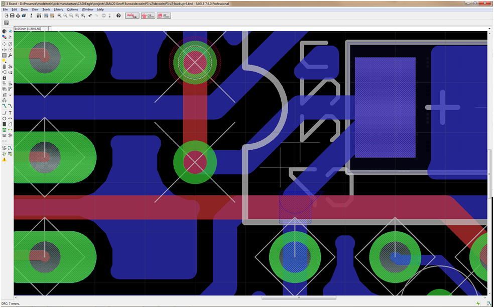
I have one single item (via) with a nasty error. I think it was originally caused by me messing around with subsequent placing then deleting a via and now I am stuck for much needed and appreciated help.
DRC gives me 7 errors, 5 on this via and 2 on one other strange place.
upload_2016-11-10_18-32-57.png


Thanks in advance, Erik
 

Attachments

  • Eagle_overlap_error.rar
    28.3 KB · Views: 200
i often get two VIAs on tip of each other. Hard to see. You can move or delete to see what is under neath the VIA.
 
Right, this was the fastest respons ever! And hit the nail on the.. : I deleted the via, and yes, one underneath it. Issue solved.

Now I still have the "overlap layer 16" error, visible to the lower right.. ??
 
Turn off the red layer. (left top "layer settings")
You will see you have two blue layers with different names connected together.
If this works hit "informative, or like". thanks
 
...
If this works hit "informative, or like". thanks


Good to know, this was new to me, thanks for pointing out!

While we are at this board: I have this ground plane drawn with the polygon technique: how do I know it is connected to ground, and where can I find/see the connection?
 
If you select the I tool and click near the lower left corner of a polygon, it shows the signal name. Any signal named "GND" as example will be connected together. Edit "name" to change the signal name if necessary.

If you select the EYE tool and click on a trace, everything in the net (i.e., the same signal name) will be highlighted.

The voice of experience says...be sure to look for islands of ground plane that are isolated from the rest of the ground plane. Things that should be connected may not be as you change the isolate distance and move things around.
 
I type into the window "polygon gnd" and that makes it so.
You can also draw a polygon and rename it gnd.

I looked at your board.
I use a board house that can do 0.007 traces. So I set the properties of the polygon to:
Width=0.007, Isolate = 0.01
This helped connect some of the grounds. (you have orphans) Pieces of ground not connected to each other.

Also you have too many blue traces and they cut up the ground. Example there is a blue on the left edge that should be red to connect ground pieced.
 
The name of the ground plane is "GND", the netclass is "1 GND". The name of all grounded tracks and pads is "AGND", the netclass is "1 GND".
I cannot change the groundplane name to "AGND":
"Signal name 'AGND' already exists!
Use the NAME command to combine signals."

When I use the "eye" symbol all AGND tracks light up, the groundplane remains dull.
 
You need to go into the edit menu and select name to rename a polygon.
 
Solved: I went to the .SCH, changed the name of a grounded wire to, say, "x", and chose the option "every segment on this sheet". Then I could go to the .brd and changed the groundplane name to "AGND". Then back to .sch and changed the grounded tracks to "AGND" with the option "every segment".
Then back to .brd, ratsnest and hopla! All ground lights up as if it were Christmas :cool:
 
Status
Not open for further replies.

Latest threads

New Articles From Microcontroller Tips

Back
Top