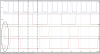
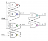
I have done a VLSI Design Layout Simulation of a D Flip-Flop. The timing diagram and schematic are as attached.
The simulation works fine and the results as desired. However I noticed, that at the timing diagram, when t=0, there seems to be a slight peaking at the output of Q' and a charge up at Q [indicated on the attached picture].
Why is this so?
The simulation works fine and the results as desired. However I noticed, that at the timing diagram, when t=0, there seems to be a slight peaking at the output of Q' and a charge up at Q [indicated on the attached picture].
Why is this so?