Continue to Site

Welcome to our site!

Electro Tech is an online community (with over 170,000 members) who enjoy talking about and building electronic circuits, projects and gadgets. To participate you need to register. Registration is free. Click here to register now.

  • Welcome to our site! Electro Tech is an online community (with over 170,000 members) who enjoy talking about and building electronic circuits, projects and gadgets. To participate you need to register. Registration is free. Click here to register now.

Curved lines in PCB design

Leaffraun-N

New Member
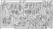
Hello, I would like to digitize and then manufacture such an old board, but I encountered a problem when choosing a program that could help me with this.
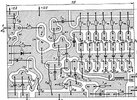
The thing is that this board (and three more auxiliary boards of this device) have non-standard curved pads for contacts.
Basically, I need to outline these pads with curved lines, and then make these curved perimeters solid (fill).
In tutorials on popular programs, I did not see anything similar to what I need. Because, in modern times, it is customary to distribute everything with ordinary angular buses.

But maybe there are other ways?

It's just... Unfortunately, I do not have enough experience in electronics to try to remake this (and other) boards in a modern way.
After all, these boards were designed by smart people, for a considerable current of a large number of transistors.

I would like to repeat exactly, for starters.
 

Attachments

  • XRecorder_Edited_20250615_03.jpg
    XRecorder_Edited_20250615_03.jpg
    3.9 MB · Views: 30
Solution
I have made boards like that many years ago. 1970s
Single sided and double-sided cost the same now. I would put the "jumpers" on the top side copper.
I did this in Paint.net just to make a point. The green is topside and replaces a jumper.
In any CAD there is an "area fill" command. The +12B is much of the rest of the board. The CAD can fill all unused areas with "+12B". It will look close to right.
1750004383021.png

One option: is to do what I did but in CAD. You will need to place all the holes and get the sizes right. Then connect up the traces. This option has many places to make errors.

Two option: Is to do it right. Start out with the schematic. Choose the right part for each part. Then start the PCB. Place each part about where...
Disclaimer: I haven't any usable experience with PCB software for this particular issue.

But - if there is PCB software out there, or PCB manufacturers that accept .svg filer or PDF files, I can propose a non-standard solution.
A drawing software called Inkscape should be perfect in order to manually trace the curves on this image.

I have many projects behind me using Inkscape as the primary graphic tool. I've used it along with spreadsheet in order to replicate (attempt) several pre-made PCB. But in my cases, there was never a need to produce the PCB.
 
You're over thinking it - just design the board with a modern PCB package, using two layers, place the components in the same places, and connect them with bottom layer thickish tracks. Apart from the ground connections, use the top layer for those, and then do a copper ground pour on the top layer.
 
Nigel - it looks to me like everything can be done with a single-sided board; no need for any copper on the component side. Did your post mean to say that the copper pour is on the bottom (typo)? If so, then . . .

Leaffraun - Please clarify your question. Are the copper traces on the same side of the board as the components, or are the the components on top and the traces on the bottom?

If the latter, then the component layout already is optimized for normal traces for all signals, and a copper pour on the same layer for GND connections. Does your software have the ability to assign a net (such as GND) to a copper pour?

ak
 
Disclaimer: I haven't any usable experience with PCB software for this particular issue.

But - if there is PCB software out there, or PCB manufacturers that accept .svg filer or PDF files, I can propose a non-standard solution.
A drawing software called Inkscape should be perfect in order to manually trace the curves on this image.

I have many projects behind me using Inkscape as the primary graphic tool. I've used it along with spreadsheet in order to replicate (attempt) several pre-made PCB. But in my cases, there was never a need to produce the PCB.
Thanks for the idea.
It seems EasyEda can import SVG when expanded. I'll try to draw the board in Fusion (more familiar) and import it.
 
Nigel - it looks to me like everything can be done with a single-sided board; no need for any copper on the component side. Did your post mean to say that the copper pour is on the bottom (typo)? If so, then . . .

Leaffraun - Please clarify your question. Are the copper traces on the same side of the board as the components, or are the the components on top and the traces on the bottom?

If the latter, then the component layout already is optimized for normal traces for all signals, and a copper pour on the same layer for GND connections. Does your software have the ability to assign a net (such as GND) to a copper pour?

ak
Hello! Thanks for your reply! Yes, it is a single sided board, with components on one side and copper traces on the other. There are 4 of these boards, and they connect to each other. I think it was all grounded to the case.
 

Attachments

  • IMG_20250615_184747.jpg
    IMG_20250615_184747.jpg
    874 KB · Views: 16
I have made boards like that many years ago. 1970s
Single sided and double-sided cost the same now. I would put the "jumpers" on the top side copper.
I did this in Paint.net just to make a point. The green is topside and replaces a jumper.
In any CAD there is an "area fill" command. The +12B is much of the rest of the board. The CAD can fill all unused areas with "+12B". It will look close to right.
1750004383021.png

One option: is to do what I did but in CAD. You will need to place all the holes and get the sizes right. Then connect up the traces. This option has many places to make errors.

Two option: Is to do it right. Start out with the schematic. Choose the right part for each part. Then start the PCB. Place each part about where it should be and start connecting the pins. At the end do area fills for the big area(s).

I probably would move the "+12B" to the top side "green" and let it fill the much of the board. Usually "GND" is most of the board. Or they share the topside.
Run the traces on the bottom side.

Before you put time into this check to see if you can get the parts. You can get 1/4 watt resistors OK but the caps are of concern. I think you might need to pick parts that you can get.
 
Solution
I have made boards like that many years ago. 1970s
Single sided and double-sided cost the same now. I would put the "jumpers" on the top side copper.
I did this in Paint.net just to make a point. The green is topside and replaces a jumper.
In any CAD there is an "area fill" command. The +12B is much of the rest of the board. The CAD can fill all unused areas with "+12B". It will look close to right.
View attachment 150156
One option: is to do what I did but in CAD. You will need to place all the holes and get the sizes right. Then connect up the traces. This option has many places to make errors.

Two option: Is to do it right. Start out with the schematic. Choose the right part for each part. Then start the PCB. Place each part about where it should be and start connecting the pins. At the end do area fills for the big area(s).

I probably would move the "+12B" to the top side "green" and let it fill the much of the board. Usually "GND" is most of the board. Or they share the topside.
Run the traces on the bottom side.

Before you put time into this check to see if you can get the parts. You can get 1/4 watt resistors OK but the caps are of concern. I think you might need to pick parts that you can get.
Thanks for the answer! Yes, there shouldn't be any problems with the parts.
 
Nigel - it looks to me like everything can be done with a single-sided board; no need for any copper on the component side. Did your post mean to say that the copper pour is on the bottom (typo)? If so, then . . .
The original is a single sided board, but any modern fab house will make a minimum of a double sided board, so you make as well take advantage of it - otherwise they are just etching all of the top side off. Moving the ground tracks to the top means there's more space on the bottom for using thicker tracks where it might be advantageous.

OP - what is the board for?.
 
A single sided board has a problem that the coper may come off the board if you mechanically stress the parts.
A double sided board will have pads on top and bottom, and most importantly there is a "via", metal tube through the board. Mechanically the board is much stronger.
1750016102885.png
 
As far as recreating the artwork, it might be easiest to draw the white areas (i.e., where copper isn't) then invert the image to make an svg. There's less extraneous marks to remove that way.
 

Latest threads

New Articles From Microcontroller Tips

Back
Top