Continue to Site

Welcome to our site!

Electro Tech is an online community (with over 170,000 members) who enjoy talking about and building electronic circuits, projects and gadgets. To participate you need to register. Registration is free. Click here to register now.

  • Welcome to our site! Electro Tech is an online community (with over 170,000 members) who enjoy talking about and building electronic circuits, projects and gadgets. To participate you need to register. Registration is free. Click here to register now.

current control (tricky one)

Status
Not open for further replies.
Thankyou again!

I assume the input voltage wont be a prob, as it wont be directly connected to the 40v side.

Now come the fun bit!!! See if i can source these easily in Australia, and attempting to draw up a circuit.
 
Yeah that would be the easiest! The regulator i cant find in digikey, i would prefer to get all from one place, to save on the sometimes exorborant international shipping prices.

Any suggestions for an online downloadable program so i can attempt to draw this up?
 
Last edited:
Sorry the regulator is available from mouser.com. Are you going to cut a PCB?

At the hobbyist level a laser printer and thermal transfer is workable. At 30A I would bulk up the traces with solder since it is unlikely that you would be getting 2+ ounce copper clad.

As to CAD packages I am only familiar with the professional ones that are not affordable to the common man :(
 
Sorry that is available from mouser. I am not familiar with the affordable PCB packages.

Are you going to make a PCB? Laser toner transfer works well enough but you should flood the 30A traces with solder since you will not be getting over 1 ounce copper clad.
 
Either a PBC made as u mention, tho i do have a friend who could do it on his CNC mill thats built for doing just this!!

Last option would be the prototype boards, with bulked up tracks as u suggest.

It should be reasonably easy to get all the connections in the right place, correct??

Also what other size caps do you suggest for the filtering?
 
you lucky dog! I have often wished I had one handy to do prototypes of boards and transformers, but i have yet to put together sufficient data to convince my boss to spring for one.

The circuit is CCM and with 33uH will probably have reasonably low ripple. A 300uF cap should be more than sufficient and a 30uF would probably work. At that point it gets to keep the high frequency circulating currents contained. one across the input and one across the output, to keep the loops as small as possible. The big input cap holds up the supply during the low voltage periods of the line cycle and the regulator will compensate for the ripple on the input cap.

It functions as a current regulator and following the app note I attached earlier you can find a off time that will keep the ripple current to 5% using the inductor you chose. That is the nice thing about a variable frequency switcher - it compensates so you do not have to worry about it so much.
 
Last edited:
I found an easy to use one!, designWorks express.

Starting to draw it up now. Dont laugh, but i dont even know how some components should be fitted hehe. inductors in series with the + ? diode the same or across + and - .... .

Once i get more done i will post for a good belly laugh!

My friend built his little 3 axis CNC from scratch, 10 years work, including the drivers for the stepper motors. awsome little machine. he has done some very intricate work with it.
 
Heres my first attempt at designing a circuit! Most likely theres a heap of problems that will let it only make smoke as it is:)

With the experienced help from here im sure we can get it to work. Just let me know what to change a little at a time.
 

Attachments

  • dc-dc psupply.JPG
    dc-dc psupply.JPG
    129.8 KB · Views: 156
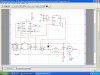
the AC source is not connected and C1 is shorted on the schematic, but since you are not making a PCB from the netlist I am sure you will be able to work around that. :)

the LD pin needs to be a voltage input from 0.5-2V for linear dimming, it actually sets the peak current. You are showing it as a simple variable resistor to GND.

R1 should be terminated to the gate pin of the IC and not to GND. this changes the regulation mode of this particular chip to peak current constant off time instead of constant frequency. this allows good regulation at duty cycles over 50%. Sorry I thought I had posted the link to the app note but it does not look like I did: https://www.electro-tech-online.com/custompdfs/2008/05/AN-H50.pdf

Early in the discussion it tells about the disadvantage of current mode regulation and explaining that constant off time takes care of it and gives figure 4. the rest of the document goes into the design formulas.

Tie U1 Vin to 18V instead of 360V. The chip is capable of running that way, but it is unnecessary dissipation when you have a lower voltage rail available. The internal linear regulator is there for running LEDs off line with out extra parts.

You do not say how you are obtaining 18V. A 12V transformer can easily reach 25V under no load conditions. 20% for regulation (small transformer spec), 20% for line variation under normal (not fault) conditions, and 40% from RMS to line peak. That is sufficient to blow U2 and the FET.

That is all I am seeing off hand.
 
Wow, i did much better than i realised:) :)

Ive added in the supply for 18V, would i be wise to keep ground isolated from the rest of the circuit?

Whats the best way to supply 0.5-2v for the LD pin? use a pot with voltage supplied from a 7805?
 
oh dear, the meter location confused me. the low side of C1 is circuit ground as well. the sense resistor goes between the FET source and GND. the output is between L3 and D2. C5, if needed (I was assuming so for noise), would be across the load.

See figure four of the app note.

That would work, but you would want at least one resistor on the high side of the pot. One on the high side and one on the low side would let you set the high and low end of the pot, realizing that the part never quite goes to zero current...

The data sheet lists a minimum on time of 450nS. I had forgotten this detail. Your off time would need to be calculated from your maximum rail level, your minimum current, and minimum drive voltage (giving you the duty cycle and hence the off time). The back through to make sure the inductor value is suitable.
 
Last edited:
Sorry I got it confused with something I was working on...the dimming pin is 0-0.25V I am working with a backlight inverter chip that is 0.5-2.5V dimming.
 
oh dear, the meter location confused me. the low side of C1 is circuit ground as well. the sense resistor goes between the FET source and GND. the output is between L3 and D2. C5, if needed (I was assuming so for noise), would be across the load.

Im a little unsure of this, i tried to draw it up as you have said to here, but something just doesnt look right.
Where does the other end of L3 go to?
 
Revision 1 :)

Ive added the 12v and 5v supplys., changed the 18V to 12V so i can run a fan from it if needed.

Moved the meter to the neg rail, as the resistance of the meter can be utilised as part of the resistance needed for current sensing, so R2 may not be needed.
Still unsure of the location of the Inductors....:confused:
 

Attachments

  • dc-dcsupply01.JPG
    dc-dcsupply01.JPG
    143.2 KB · Views: 142
Would you PLEASE look at the app note!!!! The output is ACROSS C5 and R2 is in SERIES with Q1 source
 
Last edited:
Revision 2:)

Unsure how to calculate values of R1 and R2. Theres some real heavy (complex) looking formulas in the data sheets!! Should the -output be tied into the gnd of the rest of the circuit for a feedback loop to the HV990 ?

I really appreciate all this help!!!!!
 

Attachments

  • dc-dcsupply01.JPG
    dc-dcsupply01.JPG
    143.2 KB · Views: 129
Status
Not open for further replies.

Latest threads

New Articles From Microcontroller Tips

Back
Top