Hi again,
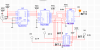
That looks pretty close although i did not check the schematic itself your wording sounds right, except for the very last line for Y7. For the state of where Y7 goes low, you have three output bits that have to go high yet you only show two connections. So you need to add one more connection to one of the NAND gates to get that last bit to go to a high during Y7.
I guess you could check the schematic in a simulation.
Also note that if we went through the Boolean logic and minimized that we may come up with a simpler solution. Im not sure if you are into doing stuff like that or not though. This would involve working with statements like:
bit 0=(AB'+A'B)*C'
or something like that (that's just a random example), one for each output bit, then trying to find the simplest solution. There is always a chance that this would lead to a simpler solution, sometimes much simpler too, but sometimes none simpler.
Last edited:
")
