Continue to Site

Welcome to our site!

Electro Tech is an online community (with over 170,000 members) who enjoy talking about and building electronic circuits, projects and gadgets. To participate you need to register. Registration is free. Click here to register now.

  • Welcome to our site! Electro Tech is an online community (with over 170,000 members) who enjoy talking about and building electronic circuits, projects and gadgets. To participate you need to register. Registration is free. Click here to register now.

Convert AGC circuit from Single to Dual Supply

Status
Not open for further replies.

Graygem

Member
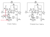
I would like to convert the single supply AGC circuit on the left, to a dual supply circuit. The right is my proposed circuit. I would appreciate your thoughts about the dual supply circuit.

I removed the R1,R5 voltage divider and grounded. I also added the negative supply.

Thank you


PrototypeAGCcontrolComparison_sm.jpg
 
What you did with the op-amp looks good.
The J-FET has problems.
Old circuit: D=1/2VI+, S=1/2VI+, G=oV
New circuit; D=0V, S=0V, G=0V. Problem is there is zero volts G to S.

I don't know what VI+ is. Pretend 10 volts.

1) If VI+=10 and VI-=-10 then: Use R1, R5, C4 to make a -5V supply and connect the ground point (R7, C5, D2) to the new -5V. This way the G to S voltage will be 5 volts again. (you moved the D and S down 5V so move the G down 5V) or 1/2 supply.

2) If VI+(old) is twice VI+(new). VI+old=10V and VI+(new)=5V, VI-=5V.
Connect the ground point (R7, C5, D2) to the new -5V. (-supply)
This way the G to S voltage will be 5 volts again. (you moved the D and S down 5V so move the G down 5V) or 1/2 supply.
upload_2014-5-8_18-26-9.png
 
I Believe their is another Problem.

Your Feedback from the Fet also needs to go to the - Input of the Op-Amp so to Reduce Gain as the signal rises.
 
I Believe their is another Problem.

Your Feedback from the Fet also needs to go to the - Input of the Op-Amp so to Reduce Gain as the signal rises.
I don't understand. "Feedback"?

The gain reduction is in the voltage divider=R4, R6, Q1.
 
I Believe the Gain Reduction in the Origional Circuit is created by the Bias voltage on Q1, via D1, changing Q1's DC Resistance and Subtracting part of the Signal via the - Input of IC1.

(Resistance of Q1 in parallel with R6, Divided by R5, feeding the AC Signal to IC1's - Input)

It is a VARIABLE GAIN Circuit.
 
Here is a Slightly Different Design.
It uses the Fet as a Variable Resistor to change the Input voltage going to the op amp.
(R6/R1+Resistance of Q1 as a Divider)

**broken link removed**
 
I Believe the Gain Reduction in the Origional Circuit is created by the Bias voltage on Q1, via D1, changing Q1's DC Resistance and Subtracting part of the Signal via the - Input of IC1.

(Resistance of Q1 in parallel with R6, Divided by R5, feeding the AC Signal to IC1's - Input)

It is a VARIABLE GAIN Circuit.

I think you're vastly over-complicating the circuit :D

The FET is simply used as the lower end of an attenuator, so no 'gain' change, simple attenuating the input to keep the output constant(ish).
 
Here is a Slightly Different Design.
It uses the Fet as a Variable Resistor to change the Input voltage going to the op amp.
(R6/R1+Resistance of Q1 as a Divider)

**broken link removed**

Isn't that almost exactly the same circuit as originally posted?, it even has the same gain resistor values.
 
If you look at the origional Single supply one, you will also see a connection from the Drain of the fet and R3 to the inverting input. It Allows for some Reduction of sound by subtracting from the origional waveform.
 
The area circled in red is the bias supply. It is 1/2 VI+. There should not be any audio at this point. This is no feed back there.
upload_2014-5-9_15-32-25.png
 

Attachments

  • upload_2014-5-9_15-31-19.png
    upload_2014-5-9_15-31-19.png
    97.6 KB · Views: 323
In my opinion, If it Were just a BIAS there would be No Reason for C2.
C2 Blocks DC bias to the IC, but allows AC Signals to go through.

The only way to know for sure would be to prototype it and check it with a scope.
 
The gain of the op-amp (with out the J-fet) is set by R3 & R2.
C2 reduces the gain to 1 at DC.

Swap C2 and R2. The function will be the same but it might look better.
 
In my opinion, If it Were just a BIAS there would be No Reason for C2.
C2 Blocks DC bias to the IC, but allows AC Signals to go through.

The only way to know for sure would be to prototype it and check it with a scope.

No reason whatsoever to do that, there is no feedback, it's just bias (opamps are simple to use and understand) - the capacitor is there simply because the high gain means that you could easily clip the amp due to the DC offset, hence a DC gain of one.
 
It is Not the DC Gain that is at Issue.
It is the AC Gain that Changes with the Signal.
 
It is Not the DC Gain that is at Issue.
It is the AC Gain that Changes with the Signal.

Obviously (although again, it's NOT the gain which changes, merely the attenuation on the input).

The DC gain IS an issue though, because if it was left without C2 the DC gain would be 200, more than enough to upset the operation of the amplifier - C2 prevents this - it's basic opamps 101.
 
If the Origional circuit uses a single supply LM358, it has a Somewhat Poor frequency response.

If you now use and TL081 or other Good Dual Supply op-amps, you will get a Better Frequency Response and Less Noise.
 
Status
Not open for further replies.

Latest threads

Back
Top