Electro Tech is an online community (with over 170,000 members) who enjoy talking about and building electronic circuits, projects and gadgets. To participate you need to register. Registration is free. Click here to register now.
Welcome to our site! Electro Tech is an online community (with over 170,000 members) who enjoy talking about and building electronic circuits, projects and gadgets. To participate you need to register. Registration is free. Click here to register now.
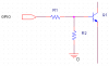
If we use BJT as a switch then we add R2 to create path to GND to avoid base from floating.
And sometimes the low level voltage is to high to ensure cut-off.
So we put R2 to proper cut-off the bjt.
R1 depends on the transistor, the collector load and the voltage source driving the base. As a rule of thumb for a low saturation voltage the base current should be 1/10th of the collector current.
Assuming the emitter goes to 0V and it's not driven an op-amp with a high, low side saturation voltage, the value of R2 is not important and is just there to speed up the switch off, improve noise immunity and minimise the leakage current.
This site uses cookies to help personalise content, tailor your experience and to keep you logged in if you register.
By continuing to use this site, you are consenting to our use of cookies.