Hi Pavan,
Disclaimer: I'm going to be honest here, and just say that although I do this for a living professionally, whatever I say is just my opinion - be it influenced by several years of experience. And like others have said, you get many differing opinions from different professionals about the same thing sometimes - and I'm still learning just like you, and will continue to learn until I kick the bucket.
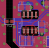
No, connecting to islands will increase your loop size. What I mean with eliminating vias around the decoupling, is to rather do something like this:
View attachment 92178
Then you pour your polygons/planes over that. It means your decoupling loop between the caps and your IC is the smallest possible, no vias in between the caps and the pins meaning your cleanest signal with the least inductance as well.
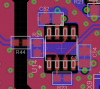
I like your improved layout with the DAC, however the split plane is still a problem in my eyes because of your single gnd pin on the DAC - however I suspected this. You have taken great care to separate your grounds, which is the absolute right method.....to begin with. Now I say, right at the end....remove the split ground pours, and combine them into one. This is good mixed signal pcb design. Yes you cannot do this with ferrite beads on the gnd returns, so rather remove your gnd ferrites - in my opinion.
I dont like a split ground plane, because you need to be ridiculously careful, and 99% of the time you just introduce much larger loops in your design.
My general rules are :
- Start with separated grounds to help you separate your digital signals, and analog signals
- Take care to put all digital sections over the digital gnd pour, and analog over the analog gnd pour
- Remove the split plane completely
The digital signals will keep to their side, and the analog sections will keep to their side, path of least impedance - preserving your signal integrity - they wont bleed into the other section. It'll be the design with the least inductive issues as well.