Continue to Site

Welcome to our site!

Electro Tech is an online community (with over 170,000 members) who enjoy talking about and building electronic circuits, projects and gadgets. To participate you need to register. Registration is free. Click here to register now.

  • Welcome to our site! Electro Tech is an online community (with over 170,000 members) who enjoy talking about and building electronic circuits, projects and gadgets. To participate you need to register. Registration is free. Click here to register now.

buck converter discontinuous mode etc

Status
Not open for further replies.

PG1995

Active Member
Hi,

I was reading the Wikipedia article on buck converter, https://en.wikipedia.org/wiki/Buck_converter , and found certain parts confusing, and need your help to clarify those with special focus on discontinuous mode.

Question 1:
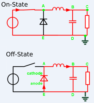
Please have a look on Figure #1 below.
1571559361500.png


During the off-state, would node A be at lower potential than the ground? For a diode, anode should be at higher potential than its cathode.

Question 2:
Under "Discontinuous Mode" section, the Wikipedia article says:

"In some cases, the amount of energy required by the load is too small. In this case, the current through the inductor falls to zero during part of the period. The only difference in the principle described above is that the inductor is completely discharged at the end of the commutation cycle (see figure 5). This has, however, some effect on the previous equations." en.wikipedia.org/wiki/Buck_converter#Discontinuous_mode

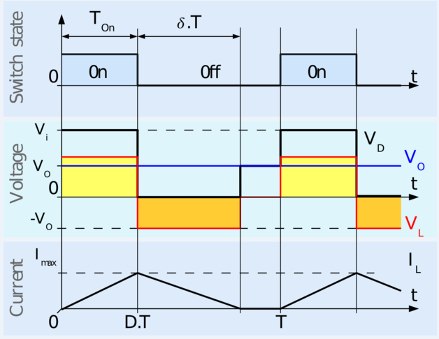
The following is my understanding of discontinuous mode. When the switch is turned off, the inductor current falls to zero; or we can say that the inductor releases all of its stored energy. The figure below does show that the inductor current falls down to zero during switch off period; the voltage across inductor, V_L, in red, also goes to zero. But I find some confusing points here.
1571559699432.png


1:
The output voltage, V_O, in blue stays constant even when inductor current falls to zero. In my opinion, this is only possible when, during off period, the current only flows around the path BCDB. No current flows through the path ABDE. Do I have it correct?

It also says:
"The inductor current falling below zero results in the discharging of the output capacitor during each cycle and therefore higher switching losses." en.wikipedia.org/wiki/Buck_converter#Discontinuous_mode

2
i :
How come the inductor current falls below zero? I thought that it only falls to zero.
ii: Does the capacitor get fully discharged? I don't think so because Vo remains almost constant as is shown in the figure above but there is a contradiction. If the capacitor does get significantly discharged then the figure shouldn't show constant output voltage Vo.

Thank you for your help!
 
Last edited:
During the off-state, would node A be at lower potential than the ground? For a diode, anode should be at higher potential than its cathode.
Yes, the voltage will be a diode drop below ground.
The output voltage, V_O, in blue stays constant even when inductor current falls to zero. In my opinion, this is only possible when, during off period, the current only flows around the path BCDB. No current flows through the path ABDE. Do I have it correct?
Yes, the capacitor is supplying the load, no current through the diode and inductor.


It also says:
"The inductor current falling below zero results in the discharging of the output capacitor during each cycle and therefore higher switching losses." en.wikipedia.org/wiki/Buck_converter#Discontinuous_mode

2
i :
How come the inductor current falls below zero? I thought that it only falls to zero.
ii: Does the capacitor get fully discharged? I don't think so because Vo remains almost constant as is shown in the figure above but there is a contradiction. If the capacitor does get significantly discharged then the figure shouldn't show constant output voltage Vo.

Thank you for your help!
To get the inductor current negative, there would have to be another switch instead of the diode, making it a synchronous buck converter. Then the inductor current would go positive and negative, charging and discharging the capacitor in each cycle. One cycle of the charge/discharge of the capacitor should not be significant enough to be shown in such simplified diagram.
 
Thank you, kubeek.

It also says:
"The inductor current falling below zero results in the discharging of the output capacitor during each cycle and therefore higher switching losses." en.wikipedia.org/wiki/Buck_converter#Discontinuous_mode

2
i :
How come the inductor current falls below zero? I thought that it only falls to zero.
ii: Does the capacitor get fully discharged? I don't think so because Vo remains almost constant as is shown in the figure above but there is a contradiction. If the capacitor does get significantly discharged then the figure shouldn't show constant output voltage Vo.

To get the inductor current negative, there would have to be another switch instead of the diode, making it a synchronous buck converter. Then the inductor current would go positive and negative, charging and discharging the capacitor in each cycle. One cycle of the charge/discharge of the capacitor should not be significant enough to be shown in such simplified diagram.

Re 2(i):
So, the inductor current could fall below zero during switch off period only in a synchronous buck converter, and this would mean that the current also flows around the path BAEDB in addition to BCDB path, and hence more discharge of capacitor.

The Wikipedia period article focuses only on asynchronous buck converter and I'd say that while saying that "The inductor current falling below zero results..." it should have at least mentioned that it's only true in case of a synchronous buck converter, and in case of a asynchronous buck converter inductor current only falls to zero.


Re 2(ii):
I don't understand where you say, "One cycle of the charge/discharge of the capacitor should not be significant enough to be shown in such simplified diagram." I believe that you are referring to capacitor voltage, Vo, which is shown to be remain constant. In my opinion, they don't show it to vary because the capacitor isn't relatively discharged much during DCM of asynchronous buck converter compared to the case of synchronous buck converter.


By the way, is there a mistake in the figure below? You can see that as soon as V_L and i_L go to zero, Vi becomes equal to Vo; notice the green rectangle. Isn't Vi the source voltage and shouldn't it remain zero during switch off period?

1571611906482.png


Could you please help me understand the underlined part?

"Discontinuous mode of conduction
The discontinuous conduction mode arises when the switching ripple in an inductor current or capacitor voltage is large enough to cause the polarity of the applied switch current or voltage to reverse, such that the current- or voltage-unidirectional assumptions made in realizing the switch with semiconductor devices are violated.
" slide #12
Source: https://www.slideshare.net/satabdyjena/buck-converter-41535853

Thanks a lot for your help!
 
Last edited:
is there a mistake in the figure below?
I think the diagram is fine.
When the switch is closed the current ramps up. Positive voltage on the inductor.
When the switch is opened the diode conducts. Current ramps down because the voltage is negative.
When current hits zero, (assuming there is no ringing) the inductor voltage and current holds at zero. You can see the voltage is at the capacitor voltage. (no voltage across the coil) With the switch open and the diode not conduction there is no where for the current to go.
 
I think the black line is Vd, not Vi. But anyway, the voltage at point A should be 0 until the new ON cycle.
 
Pretend the switch has never been on. Pretend the load is powered from an external 5 volt source. What is the voltage at point A? It should be Vout. Switch is off, Diode is off, no voltage across the inductor.
1571664772558.png

When the switch is closed Vd (black line) goes to Vin.
When the switch is first opened stored current in L forces Vd to -0.7 volts. As long as there is current in L.
When the current runs out we have voltage stored on C as Vout. With nothing happening with L, it end to end voltage drops to zero just like in the first picture.
Vd goes to Vout during (current in inductor=0) time.
1571665017800.png

Real life picture. If this was a text book the ringing would be gone and the red line is the average of that voltage.
1571665621170.png
 
Here's the LTspice simulation of a simple buck converter operating in the discontinuous mode:
(R2 and C2 form a snubber circuit to suppress the inductor oscillations that typically occur when the inductor current stops, as seen in post #7).
The MOSFET drain voltage (blue trace) goes to 10V, when the MOFSET is ON (VGS=-10V, amber trace), to the minus forward bias diode voltage, when the MOSFET is OFF and the diode is conducting (green trace) as the inductor current (red trace) flows, and then goes to the output voltage when the inductor current stops (zero volts across the inductor).
Note that the output current (purple trace) and output voltage (yellow trace) are provided by the output capacitor when the inductor current is zero.

1571695805295.png
 
Last edited:
Thank you so much!

Actually I wasn't interpreting the labels correctly. For example, the same waveform is called Vi and Vd as is shown below.

1571706561145.png


I wanted to clarify something about the the screenshot of oscilloscope. I think that the shown waveform is of voltage across the diode, Vd; and green horizontal line represents 0 V. When the current through inductor goes to zero, the voltage across diode oscillates, and when the current starts flowing through inductor, Vd jumps to input voltage Vi (the part under blue rectangular area).

1571709028170.png


1571709087498.png


This is how I understand the operation of a buck converter in discontinuous mode. The load is so light that it consumes very little power per unit time. Suppose the output is set to 5V and input is 10V, and it could vary between 4.9V and 5.1V. The switching frequency is fixed but duty cycle could be adjusted.

When the switch is turned on, the current starts flowing through inductor and the voltage starts rising across output capacitor, and the inductor also supplies current to the load directly during this period. If the load is consuming very little power, it'd take very, very little time to raise the voltage to proper voltage and then switch needs to turn off which translates into very low duty cycle. As the frequency is fixed therefore the next pulse to turn on the switch would come after a definite time interval, during this switch off period the inductor's comparatively small stored energy is used but it could last for only so long therefore capacitor also releases some of its stored energy to the load.

Please let me know if my general understanding is wrong.


Helpful links:
1:
"The inductor current falling below zero results in the discharging of the output capacitor during each cycle and therefore higher switching losses. A different control technique known as Pulse-frequency modulation can be used to minimize these losses." Source: https://en.wikipedia.org/wiki/Buck_converter#Discontinuous_mode
2: https://en.wikipedia.org/wiki/Pulse-frequency_modulation
 
Actually I wasn't interpreting the labels correctly. For example, the same waveform is called Vi and Vd as is shown below.
Actually, Vi is the voltage level corresponding to input voltage shown on the Y axis, Vd is the name for the "trace".
 
I wanted to clarify something about the the screenshot of oscilloscope.
Actually the picture is of a flyback, not a buck. I forgot to invert the picture before I posted it.
Now when the trace is high the switch is on.
When the trace is low is when the diode conducts.
In discontinuous mode, the transformer rings around the red line which is Vout.
The green line is noting.
1571774372119.png
 
Thank you very much!

Note to self:
The following video explains the operation of a flyback converter: /watch?v=HOXgOWoN0EY (insert www.youtube.com in the front).
Also check **broken link removed**

In the picture below, when switch opens, ringing would occur at node A. The voltage at node B would remain almost constant because voltage across capacitor cannot change instantaneously. In other words, we can says voltage at node A is same as node B but the ringing oscillating voltage gets superimposed over that voltage. (note to self: check ringing_inductor video)

1571897875003.png


Flyback converter:
1571896783573.png


Ringing in flyback:
**broken link removed**
 
Last edited:
Hi,

I wanted to confirm something about the oscilloscope screenshot of a flyback converter posted by ronsimpson .

The parts of waveform labelled "A" and "B" represents Off-State. During "A" part, the diode is conducting and there is ringing during "B" because the inductor current has fallen to zero. The part "C" represents On-State. Do I have it correct?

Thank you for your help!


1572407658627.png
 
Do I have it correct?
Yes.
ringing during "B" because the inductor current has fallen to zero
From the outside it looks like the current is zero.
Inside the transformer there is copper, insulation, copper. on each turn of wire. A capacitor is conductor, insulation, conductor.
Inside the transformer there is L and C. They resonate. That is why the ringing. There is current flow from the L to C and from C to L. You just can't measure it from the outside.
Any time the switch is on or the diode is on there is a "ac short" across the inductor or transformer. When all the silicon is open the inductor is free to ring.
This is like holding a bell agains a table. It will not ring. Pull the bell off the table fast and it will ring.
 
Status
Not open for further replies.

Latest threads

New Articles From Microcontroller Tips

Back
Top