Continue to Site

Welcome to our site!

Electro Tech is an online community (with over 170,000 members) who enjoy talking about and building electronic circuits, projects and gadgets. To participate you need to register. Registration is free. Click here to register now.

  • Welcome to our site! Electro Tech is an online community (with over 170,000 members) who enjoy talking about and building electronic circuits, projects and gadgets. To participate you need to register. Registration is free. Click here to register now.

Buck controller with floating driver - 2x NMOS high-side (back to back) - prevent reverse flow

Status
Not open for further replies.

ACharnley

Member
'ello!

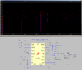
I wasn't expecting it to work because the lower FET has the charge around the gate and drain, but modifying an LTSpice example shows otherwise with the voltage drop across both being equal.

Anyone able to validate if it's a LTSpice quirk or whether it will work?
 

Attachments

  • Screenshot_2022-06-02_23-31-41.png
    Screenshot_2022-06-02_23-31-41.png
    109.9 KB · Views: 200
  • LT3740.asc
    4.8 KB · Views: 185
What "reverse flow" are you trying to prevent, that a normal buck converter does not have?
 
Indeed!

Initially I tried the dual PNP + PMOS before it but there are turn-on problems at higher current when the voltage at either side is close when factoring in ripple and the PMOS's slow resistor pulldowns. It got rather hot and became less efficient than a Schottky. If this works as well as LTSpice purports it's a nice win.
 
Since I still don't understand what you are referring to, I cannot offer any good answer to your question.
 
Ah, look at the picture, you'll see two NMOS on the high side (Q1 and Q3) and one on the low side.
Yes, I already saw that.
But you didn't answer my question as to "why"?
Normally there's just one transistor.
There is no "reverse flow" through a single transistor, so what are you trying to prevent?
You seem to be addressing a phantom problem.
 
No a NMOS has the properties of a diode with reverse flow when the voltage on the source exceeds the drain.

Why.. prevent a super capacitor discharging through the FET. Don't assume there's further diodes or a power source upstream.
 
a NMOS has the properties of a diode with reverse flow when the voltage on the source exceeds the drain.
So when does the source voltage exceed the drain voltage?
In normal operation of the buck regulator, that does not happen.
 
Okay, if you need to stop the current if power is lost (why), then the two back-to-back MOSFETs should work.
 
I had to add the diodes as LTSpice doesn't model them but it does appear to work.

Normally the back-2-back technique is around the gate and drains on both FET's, which is why I think there's potentially a problem.
 
In fact, the body diode of a high side NMOS switch does exactly what you want it to do which is to discharge the output capacitor without the necessity of a power wasting bleeder resistor, when the DC input is turned off. All of the NMOS models I have used model the body diode and you can even measure the characteristics. Here is an example of the body diode characteristic.
1654482377506.png

Can you suggest a MOSFET that will not display this characteristic?
 
Last edited:
You're the one that made the assertion that LTspice does not model the body diodes, which appears to lack credibility. In the B2B case there may be picoamperes of leakage current. The original question described a phantom problem which does not normally exist in buck converters, which behave rationally when the input power is removed. I'm still not clear on what problem you are trying to solve.

I'm also not clear on the nature of the LTspice quirk you think you have discovered.
 
Last edited:
Wouldn't it be more effective to add a FET switch between the buck converter and final load, to give total isolation from the feedback circuit and other leakage loads etc?

A static switch will need / waste less energy than driving another FET gate at high frequency.

You could add a diode and high impedance RC storage / discharge circuit to feed the switch FET gate, driven from an appropriate point on the converter, such as the upper gate driver for an N channel, or pulled down by the switch for a P channel.
 
Status
Not open for further replies.

Latest threads

New Articles From Microcontroller Tips

Back
Top