Continue to Site

Welcome to our site!

Electro Tech is an online community (with over 170,000 members) who enjoy talking about and building electronic circuits, projects and gadgets. To participate you need to register. Registration is free. Click here to register now.

  • Welcome to our site! Electro Tech is an online community (with over 170,000 members) who enjoy talking about and building electronic circuits, projects and gadgets. To participate you need to register. Registration is free. Click here to register now.

Battery Change Over Circuit Question

Status
Not open for further replies.

Mark_R

Member
Hi,

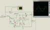
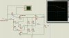
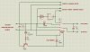
Please see attached circuit. This is a change over circuit for a battery back up in a remote data logger / transmitter. The output of this circuit feeds some small 12v loads as well as linear Vregs for 5V and 3.3V rails.

The 12V loads can take a glitch, but the regs feed a µC and modem which would reset on brownout, which can't happen.

I'm trying to figure out the size of C1 such that it could hold up the 12V rail during the time the relay drops out and transfers to battery, but I'm struggling with the math. I also am trying to figure out if the surge current when the cap recharges would exceed the 5A rating of the contacts on R1.

-The load on the output is max 24 watts 2A (max during cellular modem Tx burst, normally less)
-D1 is intended to initiate changeover when power supply drops below 9 volts
-D3 is intended to prevent C1 from helping to hold the relay engaged upon power fail
-C2 is required by the battery charger IC per their application notes.

Any thoughts on sizing C1? (as well as any other stupid ideas in this circuit) [Edit; I didn't mean your ideas would be stupid, I mean point out any of my stupid ideas]

Thanks.
 

Attachments

  • Battery Relay.jpg
    Battery Relay.jpg
    114.7 KB · Views: 263
Last edited:
The formula for the voltage drop in a capacitor is V= (I x t)/C where I is the current, t is the time and C is the capacitance.

Thus, for example, with 2A load, and a 2V drop during say 100ms for the relay to switch, the required capacitance would be (2A x 0.1s)/2V = 0.1F or 100,000µF.

You could put a small resistor in series with the cap to reduce the surge current, but remember that also reduces the output voltage of the cap by 2A x R.

Ouch! that's a big Cap!
Looking at the datasheet for the relay, they quote a 5ms release time. If I double that to 10ms for a safety factor, that's still a 10,000µF cap. Perhaps I'll ditch the relay and go with a MOSFET.
 
If you use MOSFETs, be aware that they do not block voltage in both directions due to the parasitic drain-source diode.
 
Mosfet version

This comes from the application note for the charge controller I'm using. As you can see from the scope, it works great when simulated. The load switches to battery when the power supply drops below 8≈V.

I'm confused about the MOSFET orientation however; the circuit works, and the MOSFET is oriented as in the few examples I can Google up, with the source towards positive & drain towards negative.

My confusion comes from the textbook I have handy (see scan) which appears to show the MOSFET the other way around. What gives? Is there a typo in the book, or am I missing something?

Thanks.
 

Attachments

  • MOSFET CIRCUIT.jpg
    MOSFET CIRCUIT.jpg
    209.4 KB · Views: 222
  • textbook.jpg
    textbook.jpg
    27.4 KB · Views: 196
That diagram is incorrect for a P-MOSFET. It would be correct for an N-MOSFET. (Just goes to show, you can't believe everything you see in a book).

The circuit you simulated will allow power supply current to flow through the parasitic drain-source diode in the MOSFET to the battery (its anode is connected to the drain and cathode to the source for a P-MOSFET) if the power supply voltage is two diode drops higher than the battery voltage. Is that OK?

Whoops, I forgot the diode on the battery. The diodes were also supposed to be schottkys.

How about this?

What's the purpose of the parasitic diode? Is a true diode added into the MOSFET or is it a "thoretical" diode created as part of the structure of the MOSFET. (I don't know if that question makes much sense). I see the diode symbol on the datasheets and was wondering what the deal was.

Thanks.
 

Attachments

  • MOSFET CIRCUIT.jpg
    MOSFET CIRCUIT.jpg
    195.5 KB · Views: 218
The diode is a real but unavoidable part of the normal fabrication of a MOSFET. The causes the drain-source connection to look like a diode when a voltage in reverse to the normal polarity is applied.
 
Status
Not open for further replies.

New Articles From Microcontroller Tips

Back
Top