Hi
In reply to Q2, KISS said that as the frequency gets larger, everything gets smaller such as transformers etc. Could you please tell how the size of a transformer is dependent on the frequency used? I'm sorry if I'm missing something obvious. Thanks.
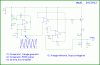
In reply to Q1, MrAl said, "Yes, or a comparator and op amp to achieve PWM". Could you please show me how this circuit will be implemented?
I understand that in n-type material, electrons are majority carriers and the holes are minority carriers. Likewise, in p-type material, the holes are majority carriers and electrons are minority carriers. But how are the majority carrier and minority carrier
devices differentiated? For instance, in a majority carrier device, majority carriers could either be electrons or holes.
It says
here that a power semiconductor device is usually used in "commutation mode" (i.e., it is either on or off), and therefore has a design optimized for such usage; it should usually not be used in linear operation
. What does it mean by "linear operation"? Perhaps, the linear operation refers to the condition where a semiconductor device keeps functioning in same state for prolonged period of time. Please help me. Thanks.
Thank you for the help.
Regards
PG