Hi,
I am doing a 4kW power supply PCB at the moment. There are a lot of footprints to make (Eagle Pro). I will have to hand solder it, and may well have to remove/replace each component multiple times in testing/evaluation.
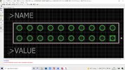
I downloaded a footprint for a connector from snapEDA….(as attached)…..as you can see, this footprint is totally unsuitable for a prototype where the part may need to be removed/replaced multiple times…the restrings are just 0.15mm….the first time this is desoldered, those pads will be ripped off.
This footprint is totally unuseable…..are there any of the free footprint providers who do footprints that are good for extensive PCB testing?…….i would say that even for a production board, a 0.15mm restring is totally unsuitable….especially where there’s room for a much bigger restring?
I am doing a 4kW power supply PCB at the moment. There are a lot of footprints to make (Eagle Pro). I will have to hand solder it, and may well have to remove/replace each component multiple times in testing/evaluation.
I downloaded a footprint for a connector from snapEDA….(as attached)…..as you can see, this footprint is totally unsuitable for a prototype where the part may need to be removed/replaced multiple times…the restrings are just 0.15mm….the first time this is desoldered, those pads will be ripped off.
This footprint is totally unuseable…..are there any of the free footprint providers who do footprints that are good for extensive PCB testing?…….i would say that even for a production board, a 0.15mm restring is totally unsuitable….especially where there’s room for a much bigger restring?