Hello,
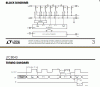
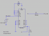
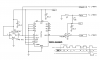
I am creating a test fixture in which I have to control, provide input digital signal into a DAC LTC8043. This DAC outputs an Iout going to the inverting input of a LT1097(op amp) which is a current to voltage converter which provides a voltage going to a LED.
My problem is that I need to control this LED which involves providing the DAC with CLK, SRI (serial digital input), and LD (load) signals.
The DAC is a 12 bit DAC, serial input.
I have selected an 8 bit Parrallel In Serial out shift register where the parrallel bits are set via DIP switches either connected HI or LOW.
How are these bits loaded into the PISO ?.
How can I load the serial output from the PISO into the DAC ?
What kind of CLK is needed ?
Also another question is:
With 8 bit serial input to the 12 bit DAC, will there be any issue with the last 4 bits in the DAC ?? Will these 4 bits become dont cares ?. Or does the DAC need exactly 12 bit input ?
Please help.
Thanks in advance for any help on this..Greatly appreciate it.