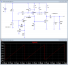
Roff, can you please explain why you chose to use that configuration of emitter follower? I mean the two PNP BJTs (Q1 & Q2) configured as shown on the image.
Q2 is being directly biased by the R10 10K resistor, also I see that C3 100nF has been added. Also, you are simulating the Rload and Cload as if they were actual loads, correct?
Regards,
-Steve.


")
