An electronic fuse eliminates fuse replacement in case of an overload and does not dissipate any power under short-circuit conditions as a current-limiter circuit would.
Shown below is a two transistor (one PNP BJT and one P-MOSFET) version of a DC, high-side electronic fuse for positive voltages.
Reversing the transistor polarities to NPN and N-MOSFET would give a high-side fuse for negative voltages.
Q1 monitors the voltage across the shunt resistor R1. When the current increases so that the voltage across R1 causes Q1 to start conducting, it raises M1's gate voltage (reducing the Vgs voltage) and turning off M1.
Since the output voltage is now lower than Q1's emitter voltage, R3 starts to conduct, which adds base current to Q1, turning it fully on and generating a latched state with M1 fully off.
The circuit stays in this latched state unit the power is shut off or the load is removed (as is done in the simulation with the test switch SReset).
M1 can be just about any P-MOSFET device with adequate voltage and ON resistance ratings.
To avoid having to heatsink the MOSFET, its ON resistance should generate an I²Ron dissipation of no more than about 1W at the current limit point.
If the voltage is below 10V then it needs to be a logic-level device (Ron specified at a Vgs of -5V or less in the data sheet).
If the voltage is above the Vgs(max) rating of the MOSFET (typically 20V) then some additional circuitry to limit Vgs is needed.
This could be as simple as a resistor added between the source and gate to act as a voltage divide and reduce the maximum Vgs.
C1 is an optional capacitor that slows the response of the circuit to eliminate nuisance tripping if that's a problem due to load start-up transients. Its value should be no higher than needed to prevent such tripping.
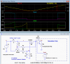
The LTspice simulation is shown for two supply voltages of 5V and 20V with the simulated load resistance varying from 30 ohms to zero and back (top trace).
The circuit trips at about 1A and the output then stays off until it is reset at 6s by the momentary closure of SReset.
The trip current can be adjusted by changing the value of R1 and approximately equals 0.6V/R1.

Shown below is a two transistor (one PNP BJT and one P-MOSFET) version of a DC, high-side electronic fuse for positive voltages.
Reversing the transistor polarities to NPN and N-MOSFET would give a high-side fuse for negative voltages.
Q1 monitors the voltage across the shunt resistor R1. When the current increases so that the voltage across R1 causes Q1 to start conducting, it raises M1's gate voltage (reducing the Vgs voltage) and turning off M1.
Since the output voltage is now lower than Q1's emitter voltage, R3 starts to conduct, which adds base current to Q1, turning it fully on and generating a latched state with M1 fully off.
The circuit stays in this latched state unit the power is shut off or the load is removed (as is done in the simulation with the test switch SReset).
M1 can be just about any P-MOSFET device with adequate voltage and ON resistance ratings.
To avoid having to heatsink the MOSFET, its ON resistance should generate an I²Ron dissipation of no more than about 1W at the current limit point.
If the voltage is below 10V then it needs to be a logic-level device (Ron specified at a Vgs of -5V or less in the data sheet).
If the voltage is above the Vgs(max) rating of the MOSFET (typically 20V) then some additional circuitry to limit Vgs is needed.
This could be as simple as a resistor added between the source and gate to act as a voltage divide and reduce the maximum Vgs.
C1 is an optional capacitor that slows the response of the circuit to eliminate nuisance tripping if that's a problem due to load start-up transients. Its value should be no higher than needed to prevent such tripping.
The LTspice simulation is shown for two supply voltages of 5V and 20V with the simulated load resistance varying from 30 ohms to zero and back (top trace).
The circuit trips at about 1A and the output then stays off until it is reset at 6s by the momentary closure of SReset.
The trip current can be adjusted by changing the value of R1 and approximately equals 0.6V/R1.