Creating an infrared (IR) communications link can be very useful. Some examples of projects which may benefit from and infrared data link are wireless control, beam breaking detection, and many others. Building this communications data link using infrared technology can be quite simple. The circuits presented here are not all-encompassing, but should serve as a good starting point for further work.
How does this IR data link work?
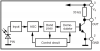
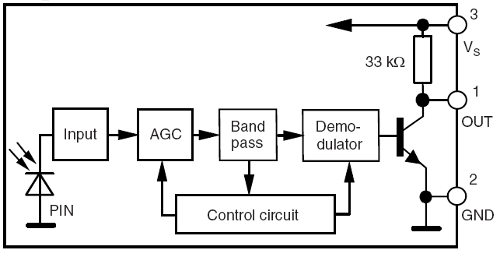
In its simplest form this IR data link works by modulating the desired data with a carrier frequency and then applying this to an emitter. The common IR receivers are designed to received an IR-specific wavelength at a specific frequency. By super-imposing the data into this frequency the IR receiver can “demodulate” (extract) the data. The IR receiver used here is the TSOP4840, and it is designed to to work with a carrier frequency of 40kHz at a wavelength of 950nm. The emitter must match this wavelength, so the high power IR diode TSAL7200 was chosen. The receiver device includes all the necessary circuitry to receive and decode the IR signal, so most of the grunt work is already done. A typical block diagram of the receiver circuitry inside the TSOP4840 is shown below.
IR Emitter Implementation:
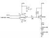
The IR emitter is implemented using the TSAL7200 IR diode. The diode is selected to match the wavelength of the receiver. Two diodes are used to provide more output power and achieve better coverage. This could of course be modified to allow for more or less coverage as required. The following figure shows the IR emitter circuit.

The logic NAND gate provides the modulation function by combining a 40kHz carrier signal with the data signal. In this way the diodes are enabled (ON) when both the carrier frequency and the data are asserted; thus the data really controls the state of the diodes. When the data is asserted the diodes will be enabled (turned ON) at the carrier frequency rate (i.e. carrier frequency will enable/disable the diodes). When the data is not asserted then diodes will be disabled (turned off), regardless of the carrier frequency state.
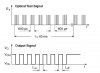
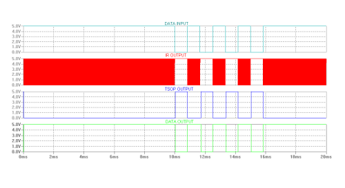
The following figure shows what these signals would look like. Notice that the data input idles at the high state. The circuit was designed with RS-232 data transmission in mind. The data input signal resembles what a typical signal would look like at the output of an MCU with a built-in UART. Also note that there are inversions throughout the signal path, but at the very end; the output data is a slightly delayed version of the input data (and the polarities are maintained).
IR Receiver Implementation:
The IR receiver is implemented using the TSOP4840 IC. This receiver matches the wavelength of the emitter diode(s). The TSOP4840 is designed to detect a 40kHz modulated IR beam. Some key factors that must be considered in using this device are as follows:
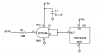
The following figure shows the IR receiver circuit.
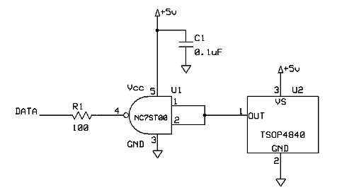
The logic NAND gate provides the inversion to make the “iddle” state of communications an active low condition; and make the “driven” state of communications an active high condition.
How does this IR data link work?
In its simplest form this IR data link works by modulating the desired data with a carrier frequency and then applying this to an emitter. The common IR receivers are designed to received an IR-specific wavelength at a specific frequency. By super-imposing the data into this frequency the IR receiver can “demodulate” (extract) the data. The IR receiver used here is the TSOP4840, and it is designed to to work with a carrier frequency of 40kHz at a wavelength of 950nm. The emitter must match this wavelength, so the high power IR diode TSAL7200 was chosen. The receiver device includes all the necessary circuitry to receive and decode the IR signal, so most of the grunt work is already done. A typical block diagram of the receiver circuitry inside the TSOP4840 is shown below.
IR Emitter Implementation:
The IR emitter is implemented using the TSAL7200 IR diode. The diode is selected to match the wavelength of the receiver. Two diodes are used to provide more output power and achieve better coverage. This could of course be modified to allow for more or less coverage as required. The following figure shows the IR emitter circuit.
The logic NAND gate provides the modulation function by combining a 40kHz carrier signal with the data signal. In this way the diodes are enabled (ON) when both the carrier frequency and the data are asserted; thus the data really controls the state of the diodes. When the data is asserted the diodes will be enabled (turned ON) at the carrier frequency rate (i.e. carrier frequency will enable/disable the diodes). When the data is not asserted then diodes will be disabled (turned off), regardless of the carrier frequency state.
The following figure shows what these signals would look like. Notice that the data input idles at the high state. The circuit was designed with RS-232 data transmission in mind. The data input signal resembles what a typical signal would look like at the output of an MCU with a built-in UART. Also note that there are inversions throughout the signal path, but at the very end; the output data is a slightly delayed version of the input data (and the polarities are maintained).
IR Receiver Implementation:
The IR receiver is implemented using the TSOP4840 IC. This receiver matches the wavelength of the emitter diode(s). The TSOP4840 is designed to detect a 40kHz modulated IR beam. Some key factors that must be considered in using this device are as follows:
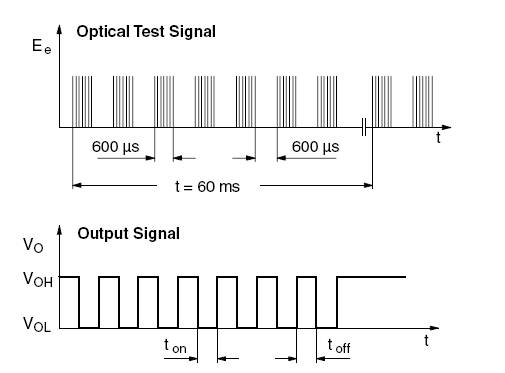
- The minimum pulse width of the modulated data must be 10 x 1/Fmod. That is to say, for the 40kHz modulation frequency, the data “on” time need to be greater than 250usec.
- The minimum gap between pulses of the modulated data must be 12 x 1/Fmod. That is to say, for the 40kHz modulation frequency, the data “off” time need to be greater than 300usec.
- From these two guidelines we can determine the maximum baud rate this device can see is 3300 or less. For typical RS232 communications, this means the maximum data rate is 2400bps.
- Data output on device “idles” high when on data (modulation) is present, and is driven “low” when data (modulation) is present.
The following figure shows the IR receiver circuit.
The logic NAND gate provides the inversion to make the “iddle” state of communications an active low condition; and make the “driven” state of communications an active high condition.