Continue to Site

Welcome to our site!

Electro Tech is an online community (with over 170,000 members) who enjoy talking about and building electronic circuits, projects and gadgets. To participate you need to register. Registration is free. Click here to register now.

  • Welcome to our site! Electro Tech is an online community (with over 170,000 members) who enjoy talking about and building electronic circuits, projects and gadgets. To participate you need to register. Registration is free. Click here to register now.

Learning about PCBs

Status
Not open for further replies.
Hello and thanks always.

So ar I have worked only with schematics and on the implementation part with breadboards and perfboards. I would like to learn the theory behind designing PCBs. I am not right now thinking of actually "making" them but learn how to design the layouts, the artwork etc. (since my knowledge is nil I dont know if I am using the correct terminology).

Can anybody advice me on links, tutorials, books or any resource for this?

For example I would like to understand the following terms:

FR-1, FR-3 CEM-3 FR-4
Surface treatement : lead-free soldering leveler, Soldering leveler , stripping beaten copper, Flux processing, Golden flash
Number of layers, Signal layer, Power supply layer
PhotoSR PrintingSR Parts surface, Solder surface
Silk
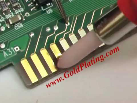
Gold platting
Board processing, v-slit processing, Perforation processing, Router processing
Artwork drawing
Garber data
RoHS, UL, CE

etc.

Thanks in advance
 
You asked many questions!
RoHS, UL, CE: These are government agencies "keep us safe". So RoHS has fools that say "no lead". UL, CE has fools that do not allow PCBs that catch on fire and kill people.

Gold platting: See the gold "connector" at the bottom of the board.
hqdefault.jpg

Silk: is the green layer that goes over the copper. Something like paint.
 
You asked many questions!
RoHS, UL, CE: These are government agencies "keep us safe". So RoHS has fools that say "no lead". UL, CE has fools that do not allow PCBs that catch on fire and kill people.

Gold platting: See the gold "connector" at the bottom of the board.

Silk: is the green layer that goes over the copper. Something like paint.

Thank you for the reply. Yes, I know it is a lot of questions but I put them so that it can be understood what I would like to learn.

All of those can be summarized in one question: Can I get a link, or book name, or resource of a tutorial where I can learn most of these concepts??

Thank you
 
I could not find it....some of the "PCB makers" have good data.
search "pcb vender"
 
Here's a tutorial on PCB layout that has been around for a few years.

David L. Jones : PCB Design Tutorial
https://alternatezone.com/electronics/files/PCBDesignTutorialRevA.pdf

A few minor corrections to Ron's comment. The green coating is called solder mask. Here's a link that discusses modern versions: https://bayareacircuits.com/an-over...nd-its-role-in-the-pcb-manufacturing-process/ The silk screen is the lettering and other comments that are printed (i.e., silk screen) onto the solder mask.

John
 
That is a pretty nice little tutorial.
 
Some terms might be Chinglish, so I;ll take a stab at some of them:
Board processing:

(Boards can be "panelized", you likely won't be doing this. For large productions runs, multiple boards are handled as one board)

v-slit processing: Exactly what it says, A slit is provided where multiple boards can be broken apart that provides a cleaner edge on the break.

Perforation processing - Think connected boards with tabs. Those tabs have holes in them to weaken the point.
You get rough edges at the tabs, but very clean ones elsewhere. Or holes where the outline should be.

Router processing - Most used for single boards, A router cuts the inside and outside cutouts
 
Status
Not open for further replies.

Latest threads

New Articles From Microcontroller Tips

Back
Top