Fluffyboii
Active Member
Greetings,
I am taking RF integrated circuit design course in my final year of university. I was strongly considering withdrawing from the class because I always felt incompetent in this topics as my ability to comprehend mathematical basics of these difficult topics run out long ago, but I did not because my friends gaslight me into thinking it was a good idea to try to pass the class anyways. Anyways I did design a LNA in the first design assignment of the class and it wasn't too difficult as it was a basic common emitter amplifier in its core.
Now I need to design a mixer and a voltage controlled oscillator to go with it. The problem is that the prof. gave no directions and just asks for few parameters to be satisfied for these devices.
VCO:
• Tuning range 6.1-7.6 GHz
• Power Consumption < 100mW
• Phase Noise < -100 dBc/Hz @ 1MHz
• Output Power > -5 dBm
You can use ideal lumped components (excluding DC block, feed etc) for ONLY VCO.
Mixer:
• RF: 6 - 7.5 GHz
• LO: 6.1 - 7.6 GHz
• IF: 0.1 GHz
• IP1dB: > -10 dBm
• NF < 15 dB
• Power Dissipation: < 150 mW
• Max Vcc: 3.3 V
• Port-to-Port Isolations: > 20 dB
This is pretty much the only info given for the assignment. I first tried utilizing my existing LNA design to convert it into a half Gilbert cell. This is the amplifier I previously designed:

I am aware that some components here are too small but that is because IHP on chip component symbols are like this. There is the simulation results:

There is the same amplifier but two of them connected to create the basic Gilbert cell:

I know that this is not a full Gilbert cell as the full cell would need 4 more transistors to have a setup like this:

For starters I wanted to see the performance of the half cell. For the differential input and outputs I have used ideal transformers to convert them to single ended ports. I matched the RF input, did not use transformer at the RF input as it is single ended because this is not a full Gilbert cell.
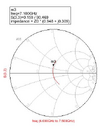
My main problem is that how do check the gain of this device. The gain of a two port device with matched input and outputs is S[21]. Which still holds as I can see that the gain of the differential pair is similar with the single amplifier I started with. But what is the definition for the gain of the current source at the bottom that is supposed to be connected to the RF input of the circuit. Looking at S parameters related to port 3 always gives absurd values about -300dB even though that port is matched.


I also tried using Design Guide of ADS to look at the Gilbert Cell of their design. I am pretty sure this is not designed to operate at 7Ghz but I did run a simulation anyways.


I can understand that the gain of the differential pair is -90dB because the circuit is not designed to work at the frequency and all but the port 3 gives similarly absurdly low values about -300dB again. I am thinking that maybe I am doing something wrong here and perhaps there is no way to judge this circuit with S parameters.

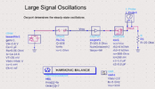
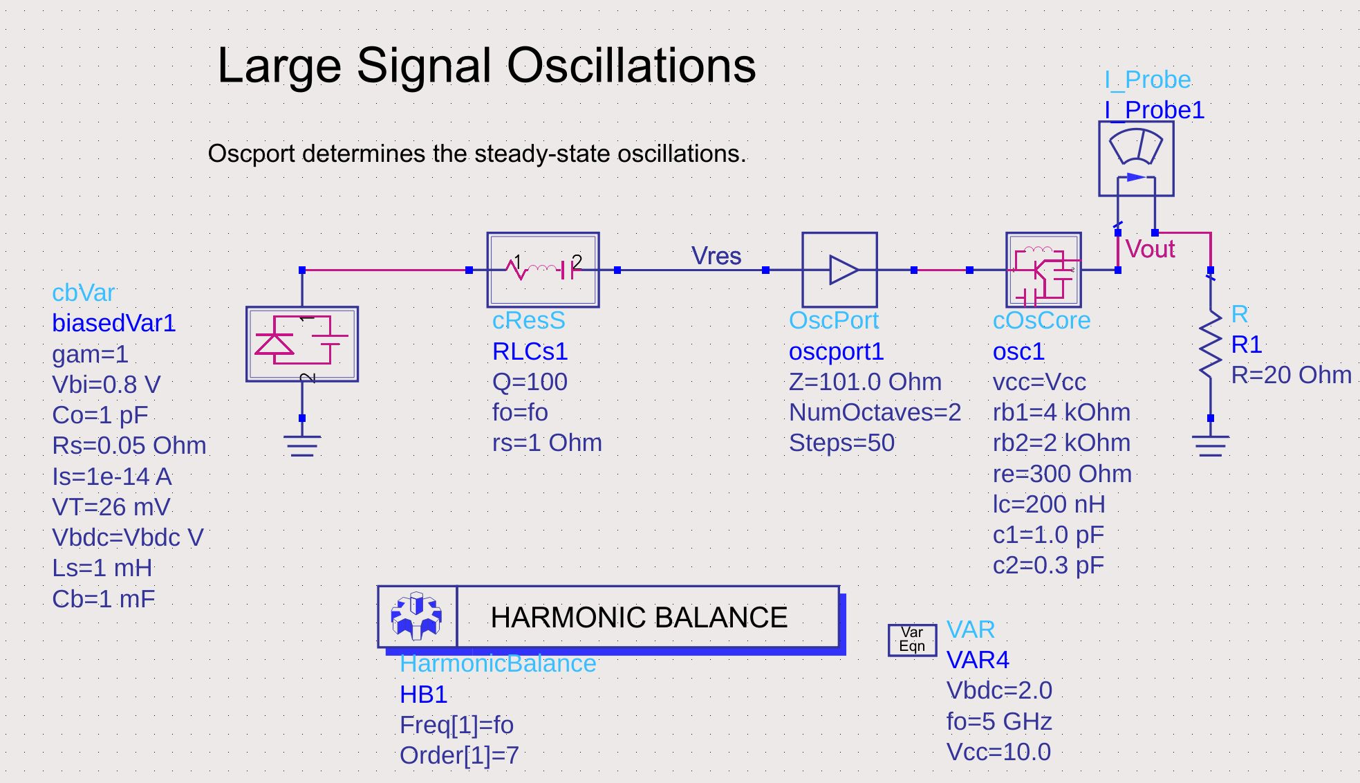
For the VCO I have no idea where to start since I don't even know if there is a Varactor in IHP library. Also the Design Guide of ADS for Oscillator is a
mystery.
I honestly have no idea how Oscillator Port works and what is cResS. The whole setup except the Oscillator Core itself, which is something like a Colpitts Oscillator doesn't make sense to me. And that is that, I have never been so lost in a assignment before. RF design never made sense to me. I would appreciate any kind of input on the topic.
I am taking RF integrated circuit design course in my final year of university. I was strongly considering withdrawing from the class because I always felt incompetent in this topics as my ability to comprehend mathematical basics of these difficult topics run out long ago, but I did not because my friends gaslight me into thinking it was a good idea to try to pass the class anyways. Anyways I did design a LNA in the first design assignment of the class and it wasn't too difficult as it was a basic common emitter amplifier in its core.
Now I need to design a mixer and a voltage controlled oscillator to go with it. The problem is that the prof. gave no directions and just asks for few parameters to be satisfied for these devices.
VCO:
• Tuning range 6.1-7.6 GHz
• Power Consumption < 100mW
• Phase Noise < -100 dBc/Hz @ 1MHz
• Output Power > -5 dBm
You can use ideal lumped components (excluding DC block, feed etc) for ONLY VCO.
Mixer:
• RF: 6 - 7.5 GHz
• LO: 6.1 - 7.6 GHz
• IF: 0.1 GHz
• IP1dB: > -10 dBm
• NF < 15 dB
• Power Dissipation: < 150 mW
• Max Vcc: 3.3 V
• Port-to-Port Isolations: > 20 dB
This is pretty much the only info given for the assignment. I first tried utilizing my existing LNA design to convert it into a half Gilbert cell. This is the amplifier I previously designed:
I am aware that some components here are too small but that is because IHP on chip component symbols are like this. There is the simulation results:
There is the same amplifier but two of them connected to create the basic Gilbert cell:
I know that this is not a full Gilbert cell as the full cell would need 4 more transistors to have a setup like this:
For starters I wanted to see the performance of the half cell. For the differential input and outputs I have used ideal transformers to convert them to single ended ports. I matched the RF input, did not use transformer at the RF input as it is single ended because this is not a full Gilbert cell.
My main problem is that how do check the gain of this device. The gain of a two port device with matched input and outputs is S[21]. Which still holds as I can see that the gain of the differential pair is similar with the single amplifier I started with. But what is the definition for the gain of the current source at the bottom that is supposed to be connected to the RF input of the circuit. Looking at S parameters related to port 3 always gives absurd values about -300dB even though that port is matched.
I also tried using Design Guide of ADS to look at the Gilbert Cell of their design. I am pretty sure this is not designed to operate at 7Ghz but I did run a simulation anyways.
I can understand that the gain of the differential pair is -90dB because the circuit is not designed to work at the frequency and all but the port 3 gives similarly absurdly low values about -300dB again. I am thinking that maybe I am doing something wrong here and perhaps there is no way to judge this circuit with S parameters.
For the VCO I have no idea where to start since I don't even know if there is a Varactor in IHP library. Also the Design Guide of ADS for Oscillator is a
mystery.
I honestly have no idea how Oscillator Port works and what is cResS. The whole setup except the Oscillator Core itself, which is something like a Colpitts Oscillator doesn't make sense to me. And that is that, I have never been so lost in a assignment before. RF design never made sense to me. I would appreciate any kind of input on the topic.