Electronic Projects, forums and more.

Go Back   Electronic Circuits Projects Diagrams Free > Electronics Forums > General Electronics Chat


General Electronics Chat This forum is for general chat about electronics, eg: Dont know what a part does? Dont know how to read a circuit? Want to get an opinion?

Reply
 
LinkBack Thread Tools Display Modes
Old 21st March 2008, 01:41 PM   (permalink)
Default EAGLE problem

Upon running DRC, I get an error, "layer abuse." Of course, no such term appears in the index nor in the two index items for layer.

Here's how I got it. I am routing a single-sided board with SMD devices on top and through-hole devices mounted on the back side with pads on the top. I realize there is an inversion there, but since all of the TH devices have the right plane of symmetry, it is no problem to remember to "flip them" when installing. For example, a TO-220 3-pin device can be shown on the top with the tab on one side and installed from the bottom with the tab on the other side.

The one exception is a 5-pin TO-220 with staggered pins (i.e., case 314B; two pins back, 3 pins forward). That is not symmetrical with respect to the plane of the tab and cannot be flipped and still work.

My solution for routing the board was to label pin 1 with a mark, mirror the device, and install it in the usual manner. The label helps me keep track of the orientation.

When the device is mirrored, EAGLE apparently thinks it goes to the bottom layer, but the pads remain on the top layer and do not have vias inserted by EAGLE, as you would see if you changed the layer of a trace. To further confuse the situation, the layer abuse error occurred for only one pin, not all 5.

Any ideas what the error means? How to avoid it? Etc. One obvious solution is to make a new device with mirrored (and mislabeled) pins, but I would like to avoid that option as I am likely to forget about the changes and get screwed in the future when I use it.

John

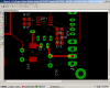
Edit: added image. The pin withthe "dot" inside the pad generates the error.
Attached Images
File Type: png Layer Abuse.PNG (84.8 KB, 25 views)

Last edited by jpanhalt; 21st March 2008 at 01:59 PM.
jpanhalt is offline  
Old 21st March 2008, 04:02 PM   (permalink)
Default

Quote:
When the device is mirrored, EAGLE apparently thinks it goes to the bottom layer, but the pads remain on the top layer and do not have vias inserted by EAGLE, as you would see if you changed the layer of a trace. To further confuse the situation, the layer abuse error occurred for only one pin, not all 5.
When a device is mirrored it switches layers. Top->Bottom or Bottom->Top.

Route the board with the SMD's on the top layer. Mirror the through hole parts when you place them, to send these component to the bottom side of the board. Through hole parts already have pads on both the top and bottom layers. No need for vias. Both the SMD and the through-hole parts will be soldered on the top layer/foil. There will be no connections to any pads on the bottom layer so you can etch it as a SS board. No need to mount parts weird.

I have never seen the layer abuse error. Would need the version of Eagle and a file to work with.
3v0 is offline  
Old 21st March 2008, 04:21 PM   (permalink)
Default

John,

Check this page: http://www.cadsoftusa.com/version41.htm

About halfway down under "DRC Command" it mentions the Layer Abuse message:

Quote:
DRC command

* The DRC now checks for objects in the Pads and Vias layer that are not Pads or Vias (i.e. wires, rectangles etc.) and flags them as "Layer Abuse" errors. The reason for this is that EAGLE does not handle these object in any special way, so they might cause short circuits. If you get such an error from the DRC, you should move the object in question into the proper signal layer(s).
Does that make any sense with what you have in your Pads or Vias layers? It's not a lot of information but it's a place to start looking, I guess. . .


Torben
Torben is offline  
Old 21st March 2008, 05:25 PM   (permalink)
Default

Gentlemen,

Both of your comments make great sense.

3v0: I put the "dot" in layer 17 (pads), but clearly, Eagle handles it slightly differently than a pad for connections. It still appears on both layers when I mirror (that's why I used layer 17), but in my version, if I click on information (eye icon) and a pad, I don't get a layer number; my dot returns the layer number.

Torben: I didn't go to the main site. I just went to Help and couldn't find it there. Thanks for taking the time to go to the main site.

As many have noted before me, most of the problems with Eagle are in just knowing where to look. Problem solved.

John
jpanhalt is offline  
Old 21st March 2008, 08:59 PM   (permalink)
Default Layer abuse

Hi jpanhalt,

I just tested if I receive that curious error message too. Parts used: 2 LM358 SMD and the rest discretes. That circuit has absolutely no practical use!

Look at the result. Routing SMDs and discretes on the top layer and also using the autorouter you must disable the bottom layer. This board was autorouted with some minor corrections for a better look.

The DRC with disabled OFF-GRID check resulted in zero errors.

Why do you mirror discretes anyway? Using the top layer only there is no need to mirror. You must mirror discretes if they have more than two pins and you intend to place them on the bottom layer.

Regards

Hans

Last edited by Boncuk; 8th July 2008 at 12:49 AM.
Boncuk is offline  
Old 21st March 2008, 10:13 PM   (permalink)
Default

Quote:
Originally Posted by Boncuk
Hi jpanhalt,

You must mirror discretes if they have more than two pins and you intend to place them on the bottom layer.
Hans
Hi Hans,

That is where the problem occurred. The device had 5 pins that were staggered. That is, unlike the typical TO-220 package with three pins in a line and in the same plane, the pins of the 5-pin device were in two parallel planes to the tab. Thus it could not be flipped and rotated to take care of the mirror imaging that occurs on the bottom layer.

As for mirroring discretes, I agree that with two pins, there is never a problem. However, with 3 or more pins, there also is not a problem if the pins are in the same plane, as they usually are with the TO-220 case.

To get the DRC error, you have to modify the package by putting a mark in layer 17 on one of the pads and then connecting to it (see my original post). Torben discovered the explanation on the Cadsoft site.

Best regards,

John
jpanhalt is offline  
Old 22nd March 2008, 05:40 AM   (permalink)
Default

The image you posted seems to indicate you are building a spot welder. Is it a project you can talk about ?
3v0 is offline  
Old 22nd March 2008, 12:31 PM   (permalink)
Default

Quote:
Originally Posted by 3v0
The image you posted seems to indicate you are building a spot welder. Is it a project you can talk about ?
It is capacitor discharge welder for battery tabs, etc. My application will be to tack weld thin-wall SS tubing together for positioning before brazing. I need a little more power than for the thinner battery tabs.

Getting a version that worked based on a link from Pommie (http://www.philpem.me.uk/elec/welder) was easy. I used an old Variac, simple rectifier, used audio capacitor, and cheap voltmeter from Harbor Freight. Got a big, surplus SCR for about $3.00.

Then, since there was nothing else to do, I started to add some bling -- a nice box, digital setting and readout, some lock-outs and sequencers, and finally a high current DC supply. The latter is done more for experience than need. The Variac works qute well, but is heavy. Had a few problems, learned a lot, and am now routing the final PCB (hopefully).

A golden shovel without a handle probably describes it best. When it is done, I would be more than happy to share pictures, schematics, and layouts with anyone who wants them. I also tried a microwave oven transformer welder. Secondary was about 6 turns of AWG 4 welding cable, used an electronic timer so I could control weld time to a few cycles (if needed), but it was not good good for these applications. More pressure is needed and there was much more heat effect.

Despite the snow today, Spring will be here soon, and these projects will be completed. John
jpanhalt is offline  
Old 22nd March 2008, 01:27 PM   (permalink)
Default

I will watch for it.
3v0 is offline  
Old 22nd March 2008, 02:48 PM   (permalink)
Default Eagle problem

Hello John,

how many degrees of heat should I send you? I've left a few over. Today's temperature was 40 degrees (Centigrade). I was busy on a construction site with no tree or sun protective device, melted almost away and drank a bucket of water.

I know about the problem mirroring packages using Eagle. I turned around a 40 pin ZIF-socket by designing an alternate package, but there was no logical picture afterwards. Using the "normal" package and mirroring it while placing (or afterwards) if behaves like any part used with Eagle.

Mirroring packages on a PCB isn't my thing anyway. Flying a model plane bears the same problems.

Your project sounds interesting to me. I don't know exactly what it is good for, but I imagine you can weld metal strips to batteries with it. I can purchase all kinds of batteries in Thailand, but when it comes to battery packs it is almost impossible to get the right one. Could I make an own battery pack using your design?

Of course making a pack cells can be soldered together, but that process reduces the life already by 50% according to the experience I've gained.

Kind regards again

Hans
Boncuk is offline  
Old 22nd March 2008, 02:53 PM   (permalink)
Default

Boncuk,

You should look at the link.

Mike.
Pommie is online now  
Old 22nd March 2008, 03:16 PM   (permalink)
Default

Quote:
Originally Posted by Boncuk
Mirroring packages on a PCB isn't my thing anyway. Flying a model plane bears the same problems.
Hi Hans,

Just imagine your head is in the airplane. No mirroring is needed.

The reason I put the mark on the pin was so I could keep track of the pins on the board. For me, it makes routing easier, as I usually do routing with only the origins, pads, vias, and airwires showing; sometimes, I add names. Knowing by the orientation where the power pins, etc. are makes it easier to see the symmetry in the routes. Otherwise there is too much clutter.

In a very early attempt, I mirrored the device, and somehow during the routing, the mirroring got negated. I could have hit the wrong key, or maybe Eagle was trying to "help" me, like Microsoft does. (I hate such help.) Fortunately, I discovered the error before constructing the board. Hence, I now put a mark on pin1 of the package.

Quote:
Your project sounds interesting to me. I don't know exactly what it is good for, but I imagine you can weld metal strips to batteries with it.
The original design in the link is for welding tabs to make battery packs. I generally solder mine using a big iron. I've had no reduction in life with NiCd or NiMH done that way. You just have to be quick and have a nicely tinned surface. I may use the welder for that too, but the real purpose is to position thin-walled tubing for brazing. I am making a large scale Pawnee PA-25 and decided to go with tubing. It is really hard to braze a free-standing cluster joint, unless you want to make a complicated jig. TIG welding in another option, but that welder is in storage.

John
jpanhalt is offline  
Old 23rd March 2008, 12:43 AM   (permalink)
Default

Quote:
Originally Posted by Pommie
Boncuk,

You should look at the link.

Mike.
Hi Mike,

I looked. Would you mind if I pep up your schematic a bit?

Boncuk
Boncuk is offline  
Old 23rd March 2008, 12:55 AM   (permalink)
Default

Hi John,

maybe that information is useful for you: WIMA Germany has developed a capacitor with 400F (400 Farad). A 500F version is under development, coming soon. The only problem with that cap is limited charging voltage. It is 10V. (higher ---> BOOM)

I guess it is not much the voltage which is decisive for welding, but the current is.

May be you decide to weld your own car body one day and it might be helpful to know about this cap.

http://www.wima.de

Hans
Boncuk is offline  
Old 23rd March 2008, 02:40 AM   (permalink)
Default

Thanks for the link to the capacitors. I didn't realize they were made that big.

I have tested 400uF to 4F and the limiting element seems to be the cables and the electrode contact. There was a surprising improvement (to me) in going from 6AWG leads to 4AWG. Raising the voltage a little helps a lot (V^2).

The major limitation to audio capacitors is their voltage. However, many are now rated at 20V continuous and 24V surge. I got a 3F pack cheaply, and it will probably be what I use in the final project. Also have 400 uF at 35 volts in a computer-grade pack, but I have not tried anything above 22V.

As for welding car bodies, I did that in the very early 1960's using the old oxy-acetylene and hammer technique. Fun, but slow. I'll stick to airplanes for now.

John
jpanhalt is offline  
Reply

Bookmarks

Thread Tools
Display Modes


Similar Threads
Title Starter Forum Replies Latest
omfg i hate Eagle dknguyen General Electronics Chat 79 12th February 2008 05:24 AM
How to properly do PCB edge connections in Eagle? toodles Electronic Projects Design/Ideas/Reviews 2 10th April 2007 11:36 PM
Eagle import/export -> Protel SE midnitrcr Electronic Projects Design/Ideas/Reviews 0 10th November 2006 09:54 PM
Keil C problem sarang1_in Micro Controllers 3 27th February 2005 06:05 AM
strange color camera problem schrodingerscat Electronic Projects Design/Ideas/Reviews 5 4th October 2003 08:25 PM


All times are GMT. The time now is 08:08 AM.


Electronic Circuits  |  Learning Electronics
Powered by vBulletin® Version 3.7.0
Copyright ©2000 - 2008, Jelsoft Enterprises Ltd.

eXTReMe Tracker