Electro Tech is an online community (with over 170,000 members) who enjoy talking about and building electronic circuits, projects and gadgets. To participate you need to register. Registration is free. Click here to register now.
Welcome to our site! Electro Tech is an online community (with over 170,000 members) who enjoy talking about and building electronic circuits, projects and gadgets. To participate you need to register. Registration is free. Click here to register now.
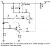
It appears to be an under-voltage / over-voltage protection circuit. If the input voltage is too low, Q1 turns on and dumps the gate of Q3 to ground. If the voltage is high enough, Q2 stops Q1 and Q3 is allowed to pass unlimited amounts of current. If the output voltage gets too high, it goes through R14 to stop Q2, which allows Q1 to make Q3 become a voltage regulator.
"If the input voltage is too low, Q1 turns on and dumps the gate of Q3 to ground."
As Q3 is a p-channel mosfet, it will turn on in this case and there will be no undervoltage protection
"If the input voltage is too low, Q1 turns on and dumps the gate of Q3 to ground."
As Q3 is a p-channel mosfet, it will turn on in this case and there will be no undervoltage protection
When positive voltage is supplied to the input, R7 makes the gate to source voltage of Q3 zero, so nothing passes.
As the input voltage increases past the 5 volts of D2 plus Vbe Q1, Q1 turns on and the gate of Q3 becomes more negative than the input voltage and Q3 turns on. Q3 passes current and the voltage divider R14 and R11 raise the emitter of Q2 to 9.1% of the output voltage.
As the input voltage increases past 10V for D1 plus Vbe Q2 plus 9.1% of Vout, Q2 turns on, which turns Q1 off. The gate of Q3 moves toward the input voltage and Q3 turns off.
This site uses cookies to help personalise content, tailor your experience and to keep you logged in if you register.
By continuing to use this site, you are consenting to our use of cookies.