Continue to Site

Welcome to our site!

Electro Tech is an online community (with over 170,000 members) who enjoy talking about and building electronic circuits, projects and gadgets. To participate you need to register. Registration is free. Click here to register now.

  • Welcome to our site! Electro Tech is an online community (with over 170,000 members) who enjoy talking about and building electronic circuits, projects and gadgets. To participate you need to register. Registration is free. Click here to register now.

Wheel of Fortune

Status
Not open for further replies.
Hello ElectroTech Forum,

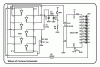
Building a child's game using a Velleman kit called Wheel of Fortune.
**broken link removed**
Have posted the schematic at
http://www.allenpitts.com/Wheel_of_Fortune_E_110126.gif
I understand how the 4017 IC works but the schematic masks the
interaction between the 4017 and the 4069 and how the 4069
makes the decade counter (4017) slow down and stop.
I am willing to offer a stipend ($50/hr) to someone who can
help me discover this knowledge.

Thanks

Allen Pitts, Dallas Texas
pittsallen@usa.net
 
The slow-down circuit consists of the top three gates, R3, D1, C2, R4 and C3.
R2 and C1 are not needed. They do nothing. They circuit has never been tested or checked.

Sw1 is pressed for a brief period.
This charges the 47u and the 1u is charged via the 100k.
The voltage on the 1u rises until it puts a HIGH on input pin 11.
This puts a LOW on pin 2 and the voltage on the 1u drops until the voltage on pin 11 is a LOW.
The HIGH on pin 2 allows the 1u to charge via the 100k and this gradually reduces the voltage on the 47u.
As the voltage on the 47u falls, the time taken to charge the 1u increases and crates the slow-down effect.
Eventually the voltage on the 1u is not enough to put a HIGH on Pin 11 and the circuit freezes.
It really only needs 2 gates and 6 components.
 
Wheel of Fortune 110131

Good evening colin55,

Thanks for the explanation.
In an effort to try to understand the relationship between the 4069 and the 4017 better
I have redrawn the schematic using the manufacturer's pin diagram. I think understand why
Velleman drew the schematic the way they did when you see the convoluted result:
Wheel_of_Fortune_F_110131.gif, attached.

I believe I am getting the idea that the slow down and eventual freesze of the circuit operation is caused
by the interaction between the 1u (C2) and 47u capacitors. I assume when you say "puts a HIGH on input pin 11."
you are talking about the pin on the 4069.

A practical condideration of adapting the circuit to the plastic chrome hubcap, Hubcap_2_21.gif
Becasue the LEDs on the kit, out of the box, are soldered to the PCB had to extend the leads to the
LEDS. Also extended the leads to the momentary switch. Tried to use a different, larger momementary
switch but the substitution made the circuit stop working. The swith which cam with the kit had
four poles where as the one i substituted only had two. Also i think the switch in the kit is
normally off and the switch I substituted were normally on. Would the ciecuit work with a two pole
switch?

If you have PayPal I would reinburse you for your time

Thanks.

Allen Pitts
469 713 4147
 

Attachments

  • Wheel_of_Fortune_F_110131.gif
    Wheel_of_Fortune_F_110131.gif
    25.5 KB · Views: 675
  • Hubcap_2_21.gif
    Hubcap_2_21.gif
    47.1 KB · Views: 449
The circuit needs an on-off switch and a push-on-switch.
The voltage on the 1u rises and falls around the mid-voltage needed by the inverter to change the state of the inverter.
The 47u is simply a weak "power supply" that gradually dies.
 
The slow-down circuit consists of the top three gates, R3, D1, C2, R4 and C3.
R2 and C1 are not needed. They do nothing. They circuit has never been tested or checked.
Incomplete, wrong, wrong, and wrong.

I know this is an old thread, but it still needs correction in case someone stumbles across it when searching for a similar circuit.

Colin's description of how the circuit functions is incorrect. R2 and C1 (and R1) are critical to its operation. Also, not only has the circuit been "tested and checked", it has been for sale around the world for many years. It works. For a discussion of how it works, here is my analysis from another forum:

That oscillator isn't what you think it is. IC1D and IC1E form a non-inverting buffer with hysteresis, which can act as a latch. It is IC1A with feedback through D1 and R2 that turns it into an oscillator. The original designer is playing some games with the resistor value ratios. For example, R1 can override the hysteresis feedback coming in through R2, and R4 might figure in there depending on the output state at pin 2.

As the overall circuit slows down, R3 always discharges C3 through D1 at the same rate. If you tied the three inverters (pins 13, 3, and 5) to pin 10 instead of the switch, then the LEDs would blink off briefly when changing from one LED to the next, and as the circuit slows down the off time would be constant and the on times would get longer and longer until the circuit stops on its final value. VERY nice.

ak
 
Oops I replied to a 6 year old thread, silly me.
 
There was a question about this type of decreasing frequency circuit on another forum. I did a search and found two threads, one where I already explained how this circuit works, and this one. I know it's an oldie, but I thought that if I tripped across it, someone else would also, so I posted an alternate theory of the crime.

ak
 
Status
Not open for further replies.

Latest threads

Back
Top