Continue to Site

Welcome to our site!

Electro Tech is an online community (with over 170,000 members) who enjoy talking about and building electronic circuits, projects and gadgets. To participate you need to register. Registration is free. Click here to register now.

  • Welcome to our site! Electro Tech is an online community (with over 170,000 members) who enjoy talking about and building electronic circuits, projects and gadgets. To participate you need to register. Registration is free. Click here to register now.

What is the difference in mechanisms in which ib1 and ib2 are formed?

Status
Not open for further replies.

hanhan

Member
Hi,
I am a bit confused about base current in BJT transistor. Please help.
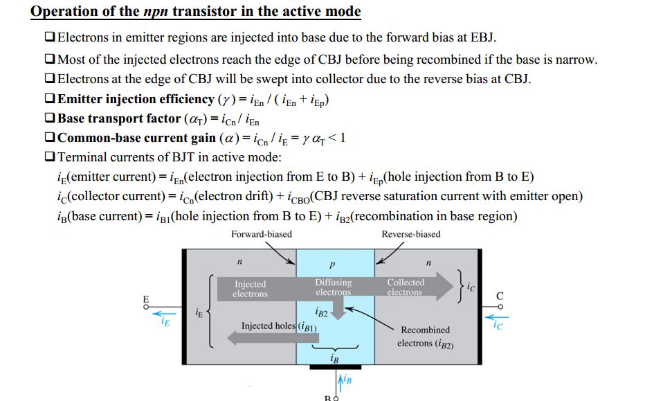
Here is a picture from a lecture.
I want to ask about iB1 (hole injection from B to E).
Holes in base are injected into emitter and then they recombined with electrons in emitter.
Are electrons in emitter that recombine with holes from base valence electrons?
If, for example, all electrons in emitter that recombine with holes from base are free electrons then
hole injected from B to E iEp will not exist, right?
base-current-1-jpg.80681
 

Attachments

  • base current 1.JPG
    base current 1.JPG
    95.3 KB · Views: 614
Anhnha,

>Holes in base are injected into emitter and then they recombined with electrons in emitter.

Injected is a poor word. Most of the current is from diffusion, with only a small amount from drift or recombination.

>Are electrons in emitter that recombine with holes from base valence electrons?

No, unlike metals, pure silicon forms a crystalline structure that uses all its 4 valance electrons to combine with 4 other silicon atoms, leaving no loosely bound electrons to wander around. That makes silicon a good insulator. When doped with a 5 valance electron element (NPN), 4 of the valance electrons combine with silicon and the 5th electron is a free electron that is available for diffusion or recombination with a hole from the base. There are also thermally generated electron-hole pairs that spontaneously form, but they are relatively few at room temperature. The same is true for regeneration-combination electron-hole pairs. So it is the free electrons that combine with the holes from the base (iB1). Unlike a metal, base valance electrons are negligible in N-type semiconductor material compared with the free electrons from the N-type material.

>If, for example, all electrons in emitter that recombine with holes from base are free electrons then
hole injected from B to E iEp will not exist, right?

I don't understand the question. What is iEp? Free electrons in the emitter that combine with holes in the base constitute only part of the emitter current. The other part is the diffusion electrons from the emitter to the base.

Ratch
 
Thank you, Ratch.
I have struggled with this for more than two days.
In the picture, emitter current contains two parts, ien and iep.
As my understanding from the picture:
ien: formed by free electrons emitted from emitter.
iep: formed by holes in base injected to emitter.
I am confused about the current iep.
iep is formed from holes moving from base to emitter; it means that holes have to move from base to emitter and in my opinion when holes move from base to emitter this is equivalent to valence electrons move from emitter to base.
>Holes in base are injected into emitter and then they recombined with electrons in emitter.

Injected is a poor word. Most of the current is from diffusion, with only a small amount from drift or recombination.
OK, I used it because this is written in the lecture too.
>Are electrons in emitter that recombine with holes from base valence electrons?

No, unlike metals, pure silicon forms a crystalline structure that uses all its 4 valance electrons to combine with 4 other silicon atoms, leaving no loosely bound electrons to wander around. That makes silicon a good insulator. When doped with a 5 valance electron element (NPN), 4 of the valance electrons combine with silicon and the 5th electron is a free electron that is available for diffusion or recombination with a hole from the base. There are also thermally generated electron-hole pairs that spontaneously form, but they are relatively few at room temperature. The same is true for regeneration-combination electron-hole pairs. So it is the free electrons that combine with the holes from the base (iB1). Unlike a metal, base valance electrons are negligible in N-type semiconductor material compared with the free electrons from the N-type material.
Sorry, I meant electrons that combined with holes from base to form iB1 not iB2.
Are these electrons valence electrons? I think they are. If not, two parts of emitter current are the same type.
>If, for example, all electrons in emitter that recombine with holes from base are free electrons then
hole injected from B to E iEp will not exist, right?

I don't understand the question. What is iEp? Free electrons in the emitter that combine with holes in the base constitute only part of the emitter current. The other part is the diffusion electrons from the emitter to the base.
iEp (now I change it to iep) is the emitter current that is formed by free electrons moving from emitter to base.
In the bold part, which base current, iB1 or iB2 do you mean in the picture?
 
Anhnha,

>Are these electrons valence electrons? I think they are. If not, two parts of emitter current are the same type.

As I said above, the silicon atoms have their valence positions filled, so there are no valence electrons like there are in metals. I don't understand your misunderstanding. Holes are diffusing from the base to the emitter and getting annihilated. Electrons are diffusing from the emitter to the base and either passing on to the collector, or a small number are getting annihilated by the holes in the base. Both the holes and electrons are contributing to the emitter current even though they are traveling in opposite directions. You can assign which is Ib1 or Ib2 from my description.

Ratch
 
Holes are diffusing from the base to the emitter and getting annihilated.
This is the part that I don't understand. If holes are annihilated in emitter, I think they recombine at the edge of emitter, then how this part contribute for emitter current?
For example, a hole is diffused from base to emitter and it recombines right away at edge of emitter by a free electron not valence electron, then this hole will not form emitter current.
 
anhnha,

>This is the part that I don't understand. If holes are annihilated in emitter, I think they recombine at the edge of emitter, then how this part contribute for emitter current?
For example, a hole is diffused from base to emitter and it recombines right away at edge of emitter by a free electron not valence electron, then this hole will not form emitter current.

It does not matter where in the emitter the hole is annihilated. The hole uses up an emitter electron to annihilate itself. Therefore, another electron can move from the emitter terminal into the emitter to produce a current.

Ratch
 
I am really confused. Please answer the question below?
In the picture, part of base current, iB1 is the flow of holes diffusing from base to emitter. After, these holes enter into emitter, electrons in emitter will recombine with these holes.
Are these electrons from valence electrons in emitter?
You said that they are free electrons but I can't understand. The reason is that if these electrons are free electrons then iB1 and iB2 are perfectly same in how these currents are formed.
In the picture, they seperate base current into two types, iB1 and iB2. Thus, I think two currents has to be different in which they are formed.
Here is my thought about how iB1 and iB2 are formed:
iB1: free electrons emitted from emitter to base and when entering into base, a very small part of these electrons recombine with holes in base and iB1 is formed.
iB2: holes diffuse from base into emitter and after entering into emitter, valence electrons in emitter will recombine with these holes and thus, new holes are created. This make holes move from base to end edge of emitter.
(in this case, I think holes move in emitter is very similar with holes moving in p type semiconductor)
 
anhnha,

>In the picture, part of base current, iB1 is the flow of holes diffusing from base to emitter. After, these holes enter into emitter, electrons in emitter will recombine with these holes.
Are these electrons from valence electrons in emitter?

Didn't I say in post #4 "...the silicon atoms have their valence positions filled, so there are no valence electrons like there are in metals"? So the electrons that annihilate the holes from the base, and the electrons that are diffused into the base are free electrons from the N-type doping element.

>You said that they are free electrons but I can't understand. The reason is that if these electrons are free electrons then iB1 and iB2 are perfectly same in how these currents are formed.

According to the picture, iB1 are the holes from the base that diffuse into the emitter and get annihilated by the free electrons in the emitter. iB2 are the electrons in the emitter that diffused into the base and are annilhilated by the holes in the base. iB1 + iB2 equal the base current. So how can iB1 be the same as iB2?

>In the picture, they seperate base current into two types, iB1 and iB2. Thus, I think two currents has to be different in which they are formed.

Yes, the two sub-currents are different. Whoever said otherwise?

>iB2: holes diffuse from base into emitter and after entering into emitter, valence electrons in emitter will recombine with these holes and thus, new holes are created. This make holes move from base to end edge of emitter.
(in this case, I think holes move in emitter is very similar with holes moving in p type semiconductor)

For the last time, there are no loosely bound valance electrons in semiconductor material like there are in metals. The bonding between the silicon-silicon and silicon-dopant is complete and tight. There are free electrons and holes in semiconductor material. Diffusion causes the movement of the holes from the base to the emitter, and the movement of the holes within the emitter. Annihilation caused by the combination in the emitter of a hole and electron does not cause a new hole to form. It does cause another hole to come from the base and another electron to come from the emitter terminal. This causes a current to exist. Holes in the N-type emitter do not last long due to the many electrons waiting to annihilate them.

Ratch
 
Status
Not open for further replies.

New Articles From Microcontroller Tips

Back
Top